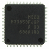
M30853FJGP#U3 Renesas Electronics America, M30853FJGP#U3 Datasheet - Page 541

M30853FJGP#U3
Manufacturer Part Number
M30853FJGP#U3
Description
IC M32C MCU FLASH 100LQFP
Manufacturer
Renesas Electronics America
Series
M16C™ M32C/80r
Datasheets
1.M3087BFLGPU3.pdf
(364 pages)
2.M30853FHFPD5.pdf
(94 pages)
3.M30853FHFPU3.pdf
(544 pages)
Specifications of M30853FJGP#U3
Core Processor
M32C/80
Core Size
16/32-Bit
Speed
32MHz
Connectivity
CAN, I²C, IEBus, SIO, UART/USART
Peripherals
DMA, WDT
Number Of I /o
85
Program Memory Size
512KB (512K x 8)
Program Memory Type
FLASH
Ram Size
24K x 8
Voltage - Supply (vcc/vdd)
3 V ~ 5.5 V
Data Converters
A/D 26x10b; D/A 2x8b
Oscillator Type
Internal
Operating Temperature
-40°C ~ 85°C
Package / Case
100-LQFP
For Use With
R0K330879S001BE - KIT DEV RSK M32C/87R0K330879S000BE - KIT DEV RSK M32C/87
Lead Free Status / RoHS Status
Lead free / RoHS Compliant
Eeprom Size
-
Available stocks
Company
Part Number
Manufacturer
Quantity
Price
Part Number:
M30853FJGP#U3M30853FJGP#D5
Manufacturer:
Renesas Electronics America
Quantity:
10 000
- Current page: 541 of 544
- Download datasheet (4Mb)
Rev.
REVISION HISTORY
Date
Page
272
273
287
290
299
300
301
302
305
310
318
320
321
322
323
324
332
333
342
351
361
365
366
368
370
373
376
385
387
399
401
Intelligent I/O
• Figure 22.1 Intelligent I/O Block Diagram BE1
• Figure 22.2 Intelligent I/O Communication Block Diagram Diagram modified
• Figure 22.13 Timer Measurement Function (1) The second condition modified
• Table 22.8 Waveform Generating Function Associated Register Settings
• Figure 22.20 G0RB and G1RB Registers Value after reset modified
• Figure 22.22 G0MR and G1MR Registers UFORM bit name changed
• Figure 22.23 G0EMR and G1EMR Registers Bit 0 modifed to RW
• Figure 22.24 G1ETC Register Bits 2 to 0 function changed
• Figure 22.27 G1IRF Register Note 2 modified
• Table 22.19 Pin Settings (4) P15
CAN Module
• Table 23.1 CAN Module Specifications Time Stamp Function specification
• Figure 23.2 Message Slot Buffer and Message Slot Diagram modified
• Table 23.2 Pin Settings P8
• Figure 23.3 C0CTLR0 and C1CTLR0 Registers Note 3 added
• 23.1.1.3 BASICCAN Bit Procedure (5) modified
• 23.1.1.6 ECRESET Bit The CAN0
• 23.1.6.5 SJW1 and SJW0 Bits Description modified
• Figure 23.9 C0BRP and C1BRP Registers Value after reset modified
• 23.1.16.1 CMOD Bit Note 1 modified
• Subsection description modified
• Subsection description modified
• Figure 23.39 Example of CAN Data Frame Receive Operation Diagram
• Figure 23.40 Operation Timing when CAN Bus Error Occurs Diagram modified
• 23.4.2.2 When the INTSEL Bit is Set to "1" Description modified
Programmable I/O Ports
• 24.3 Function Select Register Aj (PSJ Register) (i=0 to 5, 8, 9) changed to (i=0
• Figure 24.2 Programmable I/O Ports (2) Diagram modified
• Figure 24.6 P0 to P15 Registers Note 4 modified
• Figure 24.15 PUR2 Register Note 3 deleted
• Figure 24.17 IPS Register Note 2 modified
Flash Memory Version
• Figure 25.4 FMR0 Register Note 5 modified
• 25.3.3.4 FMSTP Bit Description modified
Note modified
modified
modified
to 3, 5, 8, 9)
M32C/85 Group(M32C/85, M32C/85T) Hardware Manual
C-22
Description
3
setting with the IPS register changed
OUT
Summary
2
setting with the PS9 register changed
pin on Note 2 modified to the CANi
OUT
added
OUT
pin
Related parts for M30853FJGP#U3
Image
Part Number
Description
Manufacturer
Datasheet
Request
R

Part Number:
Description:
KIT STARTER FOR M16C/29
Manufacturer:
Renesas Electronics America
Datasheet:

Part Number:
Description:
KIT STARTER FOR R8C/2D
Manufacturer:
Renesas Electronics America
Datasheet:

Part Number:
Description:
R0K33062P STARTER KIT
Manufacturer:
Renesas Electronics America
Datasheet:

Part Number:
Description:
KIT STARTER FOR R8C/23 E8A
Manufacturer:
Renesas Electronics America
Datasheet:

Part Number:
Description:
KIT STARTER FOR R8C/25
Manufacturer:
Renesas Electronics America
Datasheet:

Part Number:
Description:
KIT STARTER H8S2456 SHARPE DSPLY
Manufacturer:
Renesas Electronics America
Datasheet:

Part Number:
Description:
KIT STARTER FOR R8C38C
Manufacturer:
Renesas Electronics America
Datasheet:

Part Number:
Description:
KIT STARTER FOR R8C35C
Manufacturer:
Renesas Electronics America
Datasheet:

Part Number:
Description:
KIT STARTER FOR R8CL3AC+LCD APPS
Manufacturer:
Renesas Electronics America
Datasheet:

Part Number:
Description:
KIT STARTER FOR RX610
Manufacturer:
Renesas Electronics America
Datasheet:

Part Number:
Description:
KIT STARTER FOR R32C/118
Manufacturer:
Renesas Electronics America
Datasheet:

Part Number:
Description:
KIT DEV RSK-R8C/26-29
Manufacturer:
Renesas Electronics America
Datasheet:

Part Number:
Description:
KIT STARTER FOR SH7124
Manufacturer:
Renesas Electronics America
Datasheet:

Part Number:
Description:
KIT STARTER FOR H8SX/1622
Manufacturer:
Renesas Electronics America
Datasheet:

Part Number:
Description:
KIT DEV FOR SH7203
Manufacturer:
Renesas Electronics America
Datasheet:


