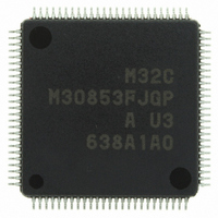
M30853FJGP#U3 Renesas Electronics America, M30853FJGP#U3 Datasheet - Page 537

M30853FJGP#U3
Manufacturer Part Number
M30853FJGP#U3
Description
IC M32C MCU FLASH 100LQFP
Manufacturer
Renesas Electronics America
Series
M16C™ M32C/80r
Datasheets
1.M3087BFLGPU3.pdf
(364 pages)
2.M30853FHFPD5.pdf
(94 pages)
3.M30853FHFPU3.pdf
(544 pages)
Specifications of M30853FJGP#U3
Core Processor
M32C/80
Core Size
16/32-Bit
Speed
32MHz
Connectivity
CAN, I²C, IEBus, SIO, UART/USART
Peripherals
DMA, WDT
Number Of I /o
85
Program Memory Size
512KB (512K x 8)
Program Memory Type
FLASH
Ram Size
24K x 8
Voltage - Supply (vcc/vdd)
3 V ~ 5.5 V
Data Converters
A/D 26x10b; D/A 2x8b
Oscillator Type
Internal
Operating Temperature
-40°C ~ 85°C
Package / Case
100-LQFP
For Use With
R0K330879S001BE - KIT DEV RSK M32C/87R0K330879S000BE - KIT DEV RSK M32C/87
Lead Free Status / RoHS Status
Lead free / RoHS Compliant
Eeprom Size
-
Available stocks
Company
Part Number
Manufacturer
Quantity
Price
Part Number:
M30853FJGP#U3M30853FJGP#D5
Manufacturer:
Renesas Electronics America
Quantity:
10 000
- Current page: 537 of 544
- Download datasheet (4Mb)
Rev.
1.01 Jan., 05
1.02 Mar., 05
REVISION HISTORY
Date
Page
465
466
473
474
477
479
114
369
371
374
414
46
68
69
82
22
24
43
54
58
68
69
• 27.5 Clock Generation Circuit Section structure modified; description modified
• Table 27.3 Power Supply Ripple added
• Figure 27.2 Power Supply Fluctuation Timing added
• 27.8 DMAC Description modified
• 27.9 Timer Ordering changed; description for Timer A modified
• 27.10 Serial I/O Ordering changed
• 27.11 A/D Converter Description modified
• Figure 27.3 Use of Capacitors to Reduce Noise Note 3 added
Reset
• Figure 5.2 Reset Sequence Figure modified
Bus
• Figure 8.3 EWCR0 to EWCR3 Registers Note 3 revised
• Table 8.5 Software Wait State and Bus Cycle EWCRi04 to EWCRi00 Bits
Clock Generation Circuit
• Figure 9.3 CM1 Register Note mark position changed
Interrupts
• Figure 11.4 Interrupt Control Register (2) Note mark position changed
Programmable I/O Port
• Figure 24.2 Programmable I/O Ports (2) Figure in Programmable I/O Ports
• Figure 24.5 PD0 to PD15 Registers Note 1 modified
• Figure 24.8 PS2 Register and PS3 Register Note 1 modified
Flash Memory Version
• Table 25.7 Pin Description (Flash Memory Standard Serial I/O Mode) De-
Memory
• Figure 3.1 Memory Map Note 3 modified
SFR
• Value after reset of the RLVL register revised
• Value after reset of the PSC register revised
Voltage Detection Circuit
• Table 6.2 Samping Time Table modified
Processor Mode
• 7.2 Setting of Pcocessor Mode description added
Bus
• Figure 8.3 EWCR0 to EWCR3 Registers Note 3 modified
• Table 8.5 Software Wait State and Bus Cycle The value “00110
with the Function Select modified
scription of P7
Register” column and “4 BCLK cycles” modified to “01010
revised
M32C/85 Group(M32C/85, M32C/85T) Hardware Manual
6
and P7
C-18
7
pins revised
Description
Summary
2
”
2
”on “EWCRi
Related parts for M30853FJGP#U3
Image
Part Number
Description
Manufacturer
Datasheet
Request
R

Part Number:
Description:
KIT STARTER FOR M16C/29
Manufacturer:
Renesas Electronics America
Datasheet:

Part Number:
Description:
KIT STARTER FOR R8C/2D
Manufacturer:
Renesas Electronics America
Datasheet:

Part Number:
Description:
R0K33062P STARTER KIT
Manufacturer:
Renesas Electronics America
Datasheet:

Part Number:
Description:
KIT STARTER FOR R8C/23 E8A
Manufacturer:
Renesas Electronics America
Datasheet:

Part Number:
Description:
KIT STARTER FOR R8C/25
Manufacturer:
Renesas Electronics America
Datasheet:

Part Number:
Description:
KIT STARTER H8S2456 SHARPE DSPLY
Manufacturer:
Renesas Electronics America
Datasheet:

Part Number:
Description:
KIT STARTER FOR R8C38C
Manufacturer:
Renesas Electronics America
Datasheet:

Part Number:
Description:
KIT STARTER FOR R8C35C
Manufacturer:
Renesas Electronics America
Datasheet:

Part Number:
Description:
KIT STARTER FOR R8CL3AC+LCD APPS
Manufacturer:
Renesas Electronics America
Datasheet:

Part Number:
Description:
KIT STARTER FOR RX610
Manufacturer:
Renesas Electronics America
Datasheet:

Part Number:
Description:
KIT STARTER FOR R32C/118
Manufacturer:
Renesas Electronics America
Datasheet:

Part Number:
Description:
KIT DEV RSK-R8C/26-29
Manufacturer:
Renesas Electronics America
Datasheet:

Part Number:
Description:
KIT STARTER FOR SH7124
Manufacturer:
Renesas Electronics America
Datasheet:

Part Number:
Description:
KIT STARTER FOR H8SX/1622
Manufacturer:
Renesas Electronics America
Datasheet:

Part Number:
Description:
KIT DEV FOR SH7203
Manufacturer:
Renesas Electronics America
Datasheet:


