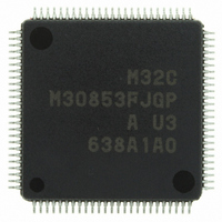
M30853FJGP#U3 Renesas Electronics America, M30853FJGP#U3 Datasheet - Page 524

M30853FJGP#U3
Manufacturer Part Number
M30853FJGP#U3
Description
IC M32C MCU FLASH 100LQFP
Manufacturer
Renesas Electronics America
Series
M16C™ M32C/80r
Datasheets
1.M3087BFLGPU3.pdf
(364 pages)
2.M30853FHFPD5.pdf
(94 pages)
3.M30853FHFPU3.pdf
(544 pages)
Specifications of M30853FJGP#U3
Core Processor
M32C/80
Core Size
16/32-Bit
Speed
32MHz
Connectivity
CAN, I²C, IEBus, SIO, UART/USART
Peripherals
DMA, WDT
Number Of I /o
85
Program Memory Size
512KB (512K x 8)
Program Memory Type
FLASH
Ram Size
24K x 8
Voltage - Supply (vcc/vdd)
3 V ~ 5.5 V
Data Converters
A/D 26x10b; D/A 2x8b
Oscillator Type
Internal
Operating Temperature
-40°C ~ 85°C
Package / Case
100-LQFP
For Use With
R0K330879S001BE - KIT DEV RSK M32C/87R0K330879S000BE - KIT DEV RSK M32C/87
Lead Free Status / RoHS Status
Lead free / RoHS Compliant
Eeprom Size
-
Available stocks
Company
Part Number
Manufacturer
Quantity
Price
Part Number:
M30853FJGP#U3M30853FJGP#D5
Manufacturer:
Renesas Electronics America
Quantity:
10 000
- Current page: 524 of 544
- Download datasheet (4Mb)
Rev.
REVISION HISTORY
Date
Page
187
188
189
195
202
203
207
209
215
216
228
238
240
244
248
250
254
255
265
266
268
270
273
274
275
276
279
• Figure 15.7 TA1MR, TA2MR, TA4 MR Registers Value after RESET
• Figure 15.8 Triangular Wave Modulation Operation revised
• Figure 15.9 Sawtooth Wave Modulation Operation revised
Serial I/O
• Figure 16.5 U0C1 to U4C1 Registers and U0SMR to U4SMR Registers
• Table 16.5 Pin Settings (3) revised
• Figure 16.10 Transmit and Receive Operation Diagram for (2) Receive
• Table 16.7 Registers to be Used and Settings in UART UiERE bit function in
• Figure 16.14 Transmit Operation revised
• Table 16.13 I
• Figure 16.20 SCLi Timing revised
• Table 16.24 Registers to be Used and Settings in GCI Mode Function of the
• Figure 16.29 SIM Interface Operation revised: Note 2 modified
• 16.7.2.1 Direct Format modified
• 16.7.2.2 Inverse Format modified
A/D Converter
• Figure 17.2 AD0CON0 Register Note 2 added
• Figure 17.6 AD0CON4 Register and AD00 to AD07 Registers Value after
• Table 17.4 Single Sweep Mode Specifications Specifications for Interrupt
• Table 17.10 Extended Analog Input Pin Settings modified
• Precautions compiled into one chapter, 25. Precautions
Intelligent I/O
• Figure 21.1 Intelligent I/O Block Diagram revised
• Figure 21.2 Intelligent I/O Communication revised
• Figure 21.4 G1BCR1 Register Note 3 added
• Figure 21.6 G1TM0 to G1TM7 Registers Note 2 added
• Table 21.1 Base Time Specifications Condition added to Base Timer Reset Con-
• Figure 21.9 Base Timer Block Diagram revised
• Figure 21.10 Counter Increment Mode revised
• Figure 21.11 Counter Increment/Decrement Mode revised
• Table 21.5 Pin Settings for Time Measurement Function P8
modified; b2 bit changed to RW reserved bit
Corrections to the UiERE bit function in the U0C1 to U4C1 registers
Timing modified
the UiC1 register modified
CLK1 to CLK0 bits in the UiC0 register modified
RESET modified
Request Generation Timing modified
dition; Counter increment/decrement mode of the Selectable Function modified
M32C/85 Group(M32C/85, M32C/85T) Hardware Manual
2
C Mode Functions Note 1 modified
C-5
Description
Summary
0
changed to P8
1
Related parts for M30853FJGP#U3
Image
Part Number
Description
Manufacturer
Datasheet
Request
R

Part Number:
Description:
KIT STARTER FOR M16C/29
Manufacturer:
Renesas Electronics America
Datasheet:

Part Number:
Description:
KIT STARTER FOR R8C/2D
Manufacturer:
Renesas Electronics America
Datasheet:

Part Number:
Description:
R0K33062P STARTER KIT
Manufacturer:
Renesas Electronics America
Datasheet:

Part Number:
Description:
KIT STARTER FOR R8C/23 E8A
Manufacturer:
Renesas Electronics America
Datasheet:

Part Number:
Description:
KIT STARTER FOR R8C/25
Manufacturer:
Renesas Electronics America
Datasheet:

Part Number:
Description:
KIT STARTER H8S2456 SHARPE DSPLY
Manufacturer:
Renesas Electronics America
Datasheet:

Part Number:
Description:
KIT STARTER FOR R8C38C
Manufacturer:
Renesas Electronics America
Datasheet:

Part Number:
Description:
KIT STARTER FOR R8C35C
Manufacturer:
Renesas Electronics America
Datasheet:

Part Number:
Description:
KIT STARTER FOR R8CL3AC+LCD APPS
Manufacturer:
Renesas Electronics America
Datasheet:

Part Number:
Description:
KIT STARTER FOR RX610
Manufacturer:
Renesas Electronics America
Datasheet:

Part Number:
Description:
KIT STARTER FOR R32C/118
Manufacturer:
Renesas Electronics America
Datasheet:

Part Number:
Description:
KIT DEV RSK-R8C/26-29
Manufacturer:
Renesas Electronics America
Datasheet:

Part Number:
Description:
KIT STARTER FOR SH7124
Manufacturer:
Renesas Electronics America
Datasheet:

Part Number:
Description:
KIT STARTER FOR H8SX/1622
Manufacturer:
Renesas Electronics America
Datasheet:

Part Number:
Description:
KIT DEV FOR SH7203
Manufacturer:
Renesas Electronics America
Datasheet:


