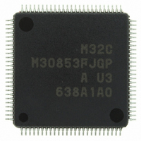
M30853FJGP#U3 Renesas Electronics America, M30853FJGP#U3 Datasheet - Page 91

M30853FJGP#U3
Manufacturer Part Number
M30853FJGP#U3
Description
IC M32C MCU FLASH 100LQFP
Manufacturer
Renesas Electronics America
Series
M16C™ M32C/80r
Datasheets
1.M3087BFLGPU3.pdf
(364 pages)
2.M30853FHFPD5.pdf
(94 pages)
3.M30853FHFPU3.pdf
(544 pages)
Specifications of M30853FJGP#U3
Core Processor
M32C/80
Core Size
16/32-Bit
Speed
32MHz
Connectivity
CAN, I²C, IEBus, SIO, UART/USART
Peripherals
DMA, WDT
Number Of I /o
85
Program Memory Size
512KB (512K x 8)
Program Memory Type
FLASH
Ram Size
24K x 8
Voltage - Supply (vcc/vdd)
3 V ~ 5.5 V
Data Converters
A/D 26x10b; D/A 2x8b
Oscillator Type
Internal
Operating Temperature
-40°C ~ 85°C
Package / Case
100-LQFP
For Use With
R0K330879S001BE - KIT DEV RSK M32C/87R0K330879S000BE - KIT DEV RSK M32C/87
Lead Free Status / RoHS Status
Lead free / RoHS Compliant
Eeprom Size
-
Available stocks
Company
Part Number
Manufacturer
Quantity
Price
Part Number:
M30853FJGP#U3M30853FJGP#D5
Manufacturer:
Renesas Electronics America
Quantity:
10 000
- Current page: 91 of 544
- Download datasheet (4Mb)
M
R
R
e
E
3
. v
J
2
Figure 8.2 Address Bus and Chip-Select Signal Outputs (Separate Bus)
0
C
1
9
0 .
8 /
B
0
3
5
Chip-Select Signal
0
Chip-Select Signal
Chip-Select Signal
3
G
J
7
u
o r
Example 3:
0 -
. l
Address Bus
Example 1:
u
0
1
Address Bus
When the microcomputer accesses the external
space j specified by another chip-select signal in the
next cycle after having accessed the external space i,
both address bus and chip-select signal change.
p
, 1
0
When the microcomputer accesses the space i
specified by the same chip-select signal in the next
cycle after having accessed the external space i,
the address bus changes but the chip-select signal
does not.
Data Bus
NOTES:
i = 0 to 3
j = 0 to 3, excluding i
(See Figure 7.3 for i, j and p, k)
i = 0 to 3
(See Figure 7.3 for i and k)
3
(
Data Bus
2
M
1. The above applies to the address bus and chip-select signal in two consecutive cycles.
0
3
CSk
0
5
2
CSp
CSk
By combining these examples, a chip-select signal extended by two or more cycles may be output.
C
8 /
Page 66
, 5
M
3
2
C
Address
f o
Access
External
Space i
8 /
Address
Access
External
Space i
k = 0 to 3
p= 0 to 3, excluding k
k = 0 to 3
4
5
9
Data
) T
4
Data
Access
External
Space i
Access
External
Space j
Data
Data
Example 4:
Chip-Select Signal
Example 2:
Chip-Select Signal
When the microcomputer accesses the SFR or the
internal ROM/RAM area in the next cycle after
having accessed an external space, the chip-select
signal changes but the address bus does not.
When the microcomputer does not access any
space in the next cycle after having accessed an
external space (no pre-fetch of an instruction is
generated), neither address bus nor chip-select
signal changes.
Address Bus
Address Bus
Data Bus
Data Bus
CSk
CSk
k = 0 to 3
k = 0 to 3
Access
External
Space
Access
External
Space
Address
Address
Data
Data
No Access
Access SFR,
Internal
ROM/RAM
Area
8. Bus
Related parts for M30853FJGP#U3
Image
Part Number
Description
Manufacturer
Datasheet
Request
R

Part Number:
Description:
KIT STARTER FOR M16C/29
Manufacturer:
Renesas Electronics America
Datasheet:

Part Number:
Description:
KIT STARTER FOR R8C/2D
Manufacturer:
Renesas Electronics America
Datasheet:

Part Number:
Description:
R0K33062P STARTER KIT
Manufacturer:
Renesas Electronics America
Datasheet:

Part Number:
Description:
KIT STARTER FOR R8C/23 E8A
Manufacturer:
Renesas Electronics America
Datasheet:

Part Number:
Description:
KIT STARTER FOR R8C/25
Manufacturer:
Renesas Electronics America
Datasheet:

Part Number:
Description:
KIT STARTER H8S2456 SHARPE DSPLY
Manufacturer:
Renesas Electronics America
Datasheet:

Part Number:
Description:
KIT STARTER FOR R8C38C
Manufacturer:
Renesas Electronics America
Datasheet:

Part Number:
Description:
KIT STARTER FOR R8C35C
Manufacturer:
Renesas Electronics America
Datasheet:

Part Number:
Description:
KIT STARTER FOR R8CL3AC+LCD APPS
Manufacturer:
Renesas Electronics America
Datasheet:

Part Number:
Description:
KIT STARTER FOR RX610
Manufacturer:
Renesas Electronics America
Datasheet:

Part Number:
Description:
KIT STARTER FOR R32C/118
Manufacturer:
Renesas Electronics America
Datasheet:

Part Number:
Description:
KIT DEV RSK-R8C/26-29
Manufacturer:
Renesas Electronics America
Datasheet:

Part Number:
Description:
KIT STARTER FOR SH7124
Manufacturer:
Renesas Electronics America
Datasheet:

Part Number:
Description:
KIT STARTER FOR H8SX/1622
Manufacturer:
Renesas Electronics America
Datasheet:

Part Number:
Description:
KIT DEV FOR SH7203
Manufacturer:
Renesas Electronics America
Datasheet:


