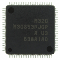
M30853FJGP#U3 Renesas Electronics America, M30853FJGP#U3 Datasheet - Page 520

M30853FJGP#U3
Manufacturer Part Number
M30853FJGP#U3
Description
IC M32C MCU FLASH 100LQFP
Manufacturer
Renesas Electronics America
Series
M16C™ M32C/80r
Datasheets
1.M3087BFLGPU3.pdf
(364 pages)
2.M30853FHFPD5.pdf
(94 pages)
3.M30853FHFPU3.pdf
(544 pages)
Specifications of M30853FJGP#U3
Core Processor
M32C/80
Core Size
16/32-Bit
Speed
32MHz
Connectivity
CAN, I²C, IEBus, SIO, UART/USART
Peripherals
DMA, WDT
Number Of I /o
85
Program Memory Size
512KB (512K x 8)
Program Memory Type
FLASH
Ram Size
24K x 8
Voltage - Supply (vcc/vdd)
3 V ~ 5.5 V
Data Converters
A/D 26x10b; D/A 2x8b
Oscillator Type
Internal
Operating Temperature
-40°C ~ 85°C
Package / Case
100-LQFP
For Use With
R0K330879S001BE - KIT DEV RSK M32C/87R0K330879S000BE - KIT DEV RSK M32C/87
Lead Free Status / RoHS Status
Lead free / RoHS Compliant
Eeprom Size
-
Available stocks
Company
Part Number
Manufacturer
Quantity
Price
Part Number:
M30853FJGP#U3M30853FJGP#D5
Manufacturer:
Renesas Electronics America
Quantity:
10 000
- Current page: 520 of 544
- Download datasheet (4Mb)
0.20
0.30
Rev.
Jan., 03
Dec., 03
REVISION HISTORY
Date
All Pages New chapters added
7, 11, 12
24 - 45
44, 45
Page
2, 3
23
46
47
48
49
50
51
52
4
5
6
New Document
Chapter, Table and Figure numbers modified
Chapter sequence modified
Overview
• Table 1.1 and 1.2 M32C/85 Group Performance
• Figure 1.1 M32C/85 Group Block Diagram Note 2 deleted
• Figure 1.2 ROM/RAM Capacity, Table 1.3 M32C/85 Group modified
• Table 1.3 M32C/85 Group Note1 deleted
• Figure 1.3 Product Numbering System ROM capacity modified
• Figure 1.4 Pin Assignment for 144-Pin Package, Figure 1.5 and 1.6 Pin As-
Memory
• Figure 3.1 Memory Map modified
SFR
• “X: Nothing is assigned” modified to “X: Indeterminate”
• “?: Indeterminate” modified to “X: Indeterminate”
• “Users cannot use any symbols with *” deleted
• Register names, symbols, value after RESET of addresses 001F
• Value after RESET of CM0, PM2, PLC0, PLC1, EWCR0 to EWCR3, RLVL,
• Annotations added within SFR list
Reset
• 5.1.1 Hardware Reset 1 New information added
• 5.2 Software Reset, Watchdog Timer Reset Reference added
• Figure 5.2 Reset Sequence Figure modified; note 1 added
• Table 5.1 Pin States Notes 2 and 3 added; P5
• 5.5 Voltage Detection Circuit New information added
• Figure 5.5 WDC Register and VCR1 Register Watchdog Timer Control Regis-
• Figure 5.6 VCR2 Register NOTES modified
“Option” deleted from Serial I/O, I
“Oscillation Stop Detect Function” added
signment for 100-Pin Package
Annotation added: P7
002B
IIO0IR to IIO5IR, IIO8IR to IIO11IR, IIO0IE to IIO5IE, IIO8IE to IIO11IE, G0CR,
G1CR, G1POCR, IPSA, C0MDR, C1MDR, C0CTLR1, C1CTLR, IDB0, IDB1,
TA0MR to TA4MR, DM0SL to DM3SL, AD00, AD0CON2, and AD0CON3 regis-
ters revised
ter added
16
, 0030
M32C/85 Group(M32C/85, M32C/85T) Hardware Manual
16
to 0035
0
C-1
and P7
16
, 0054
Description
1
16
are ports for the N-channel open drain input.
2
, and 0056
Summary
C bus, and IEBus
16
deleted
6
pin state modified
16
to 0025
16
,
Related parts for M30853FJGP#U3
Image
Part Number
Description
Manufacturer
Datasheet
Request
R

Part Number:
Description:
KIT STARTER FOR M16C/29
Manufacturer:
Renesas Electronics America
Datasheet:

Part Number:
Description:
KIT STARTER FOR R8C/2D
Manufacturer:
Renesas Electronics America
Datasheet:

Part Number:
Description:
R0K33062P STARTER KIT
Manufacturer:
Renesas Electronics America
Datasheet:

Part Number:
Description:
KIT STARTER FOR R8C/23 E8A
Manufacturer:
Renesas Electronics America
Datasheet:

Part Number:
Description:
KIT STARTER FOR R8C/25
Manufacturer:
Renesas Electronics America
Datasheet:

Part Number:
Description:
KIT STARTER H8S2456 SHARPE DSPLY
Manufacturer:
Renesas Electronics America
Datasheet:

Part Number:
Description:
KIT STARTER FOR R8C38C
Manufacturer:
Renesas Electronics America
Datasheet:

Part Number:
Description:
KIT STARTER FOR R8C35C
Manufacturer:
Renesas Electronics America
Datasheet:

Part Number:
Description:
KIT STARTER FOR R8CL3AC+LCD APPS
Manufacturer:
Renesas Electronics America
Datasheet:

Part Number:
Description:
KIT STARTER FOR RX610
Manufacturer:
Renesas Electronics America
Datasheet:

Part Number:
Description:
KIT STARTER FOR R32C/118
Manufacturer:
Renesas Electronics America
Datasheet:

Part Number:
Description:
KIT DEV RSK-R8C/26-29
Manufacturer:
Renesas Electronics America
Datasheet:

Part Number:
Description:
KIT STARTER FOR SH7124
Manufacturer:
Renesas Electronics America
Datasheet:

Part Number:
Description:
KIT STARTER FOR H8SX/1622
Manufacturer:
Renesas Electronics America
Datasheet:

Part Number:
Description:
KIT DEV FOR SH7203
Manufacturer:
Renesas Electronics America
Datasheet:


