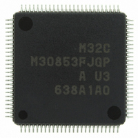
M30853FJGP#U3 Renesas Electronics America, M30853FJGP#U3 Datasheet - Page 434

M30853FJGP#U3
Manufacturer Part Number
M30853FJGP#U3
Description
IC M32C MCU FLASH 100LQFP
Manufacturer
Renesas Electronics America
Series
M16C™ M32C/80r
Datasheets
1.M3087BFLGPU3.pdf
(364 pages)
2.M30853FHFPD5.pdf
(94 pages)
3.M30853FHFPU3.pdf
(544 pages)
Specifications of M30853FJGP#U3
Core Processor
M32C/80
Core Size
16/32-Bit
Speed
32MHz
Connectivity
CAN, I²C, IEBus, SIO, UART/USART
Peripherals
DMA, WDT
Number Of I /o
85
Program Memory Size
512KB (512K x 8)
Program Memory Type
FLASH
Ram Size
24K x 8
Voltage - Supply (vcc/vdd)
3 V ~ 5.5 V
Data Converters
A/D 26x10b; D/A 2x8b
Oscillator Type
Internal
Operating Temperature
-40°C ~ 85°C
Package / Case
100-LQFP
For Use With
R0K330879S001BE - KIT DEV RSK M32C/87R0K330879S000BE - KIT DEV RSK M32C/87
Lead Free Status / RoHS Status
Lead free / RoHS Compliant
Eeprom Size
-
Available stocks
Company
Part Number
Manufacturer
Quantity
Price
Part Number:
M30853FJGP#U3M30853FJGP#D5
Manufacturer:
Renesas Electronics America
Quantity:
10 000
- Current page: 434 of 544
- Download datasheet (4Mb)
R
R
M
e
E
3
. v
J
2
Figure 25.10 Block Erase Command
0
C
1
9
0 .
B
8 /
0
3
25.3.5.5 Block Erase Command
5
0
The block erase command erases each block.
Auto erase operation (erase and verify) will start in the specified block by writing command code
"xx20
bus cycle.
The FMR00 bit in the FMR0 register indicates whether or not an auto erase operation has been
completed. The FMR00 bit is set to "0" (busy) during auto erase and to "1" (ready) when the auto
erase operation is completed.
After the completion of an auto erase operation, the FMR07 bit in the FMR0 register indicates whether
or not the auto erase operation has been completed as expected. (Refer to 25.3.8 Full Status
Check.)
Figure 25.10 shows a flow chart of the block erase command programming.
The lock bit can protect each block from being programmed inadvertently. (Refer to 25.3.6 Data
Protect Function.)
In EW mode 1, do not execute this command on the block where the rewrite control program is allocated.
In EW mode 0, the microcomputer enters read status register mode as soon as an auto erase opera-
tion starts. The SRD register can be read. The SR7 bit in the SRD register is set to "0" at the same
time an auto erase operation starts. It is set to "1" when an auto erase operation is completed. The
microcomputer remains in read status register mode until the read array command or read lock bit
status command is written.
3
J
G
7
u
o r
0 -
. l
u
0
1
, 1
0
p
16
3
(
2
" in the first bus cycle and "xxD0
M
0
0
3
5
2
C
8 /
Page 409
, 5
M
NOTES:
3
1. Write the command code and data to even addresses.
2
C
f o
8 /
4
5
9
) T
4
Write the command code "xx20
Write "xxD0
Block erase operation
16
order block address
Full status check
" to the highest-order even address of a block in the second
is completed
FMR00=1?
16
Start
" to the highest-
YES
NO
16
"
25. Flash Memory Version
Related parts for M30853FJGP#U3
Image
Part Number
Description
Manufacturer
Datasheet
Request
R

Part Number:
Description:
KIT STARTER FOR M16C/29
Manufacturer:
Renesas Electronics America
Datasheet:

Part Number:
Description:
KIT STARTER FOR R8C/2D
Manufacturer:
Renesas Electronics America
Datasheet:

Part Number:
Description:
R0K33062P STARTER KIT
Manufacturer:
Renesas Electronics America
Datasheet:

Part Number:
Description:
KIT STARTER FOR R8C/23 E8A
Manufacturer:
Renesas Electronics America
Datasheet:

Part Number:
Description:
KIT STARTER FOR R8C/25
Manufacturer:
Renesas Electronics America
Datasheet:

Part Number:
Description:
KIT STARTER H8S2456 SHARPE DSPLY
Manufacturer:
Renesas Electronics America
Datasheet:

Part Number:
Description:
KIT STARTER FOR R8C38C
Manufacturer:
Renesas Electronics America
Datasheet:

Part Number:
Description:
KIT STARTER FOR R8C35C
Manufacturer:
Renesas Electronics America
Datasheet:

Part Number:
Description:
KIT STARTER FOR R8CL3AC+LCD APPS
Manufacturer:
Renesas Electronics America
Datasheet:

Part Number:
Description:
KIT STARTER FOR RX610
Manufacturer:
Renesas Electronics America
Datasheet:

Part Number:
Description:
KIT STARTER FOR R32C/118
Manufacturer:
Renesas Electronics America
Datasheet:

Part Number:
Description:
KIT DEV RSK-R8C/26-29
Manufacturer:
Renesas Electronics America
Datasheet:

Part Number:
Description:
KIT STARTER FOR SH7124
Manufacturer:
Renesas Electronics America
Datasheet:

Part Number:
Description:
KIT STARTER FOR H8SX/1622
Manufacturer:
Renesas Electronics America
Datasheet:

Part Number:
Description:
KIT DEV FOR SH7203
Manufacturer:
Renesas Electronics America
Datasheet:


