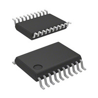
R5F21324CNSP#U0 Renesas Electronics America, R5F21324CNSP#U0 Datasheet - Page 171

R5F21324CNSP#U0
Manufacturer Part Number
R5F21324CNSP#U0
Description
MCU 1KB FLASH 16K ROM 20-LSSOP
Manufacturer
Renesas Electronics America
Series
R8C/3x/32Cr
Datasheet
1.R5F21321CDSPU0.pdf
(605 pages)
Specifications of R5F21324CNSP#U0
Core Processor
R8C
Core Size
16/32-Bit
Speed
20MHz
Connectivity
I²C, LIN, SIO, SSU, UART/USART
Peripherals
POR, PWM, Voltage Detect, WDT
Number Of I /o
15
Program Memory Size
16KB (16K x 8)
Program Memory Type
FLASH
Ram Size
1.5K x 8
Voltage - Supply (vcc/vdd)
1.8 V ~ 5.5 V
Data Converters
A/D 4x10b
Oscillator Type
Internal
Operating Temperature
-20°C ~ 85°C
Package / Case
20-LSSOP
Lead Free Status / RoHS Status
Lead free / RoHS Compliant
Eeprom Size
-
- Current page: 171 of 605
- Download datasheet (6Mb)
R8C/32C Group
REJ09B0573-0100 Rev.1.00 Dec. 18, 2009
Page 142 of 573
11.6
Table 11.8
Notes:
Table 11.9
• Instruction with 2-byte operation code
• Instruction with 1-byte operation code
ADD.B:S
OR.B:S
STNZ
CMP.B:S
JMPS
MOV.B:S
Instructions other than above
Address match interrupt 0
Address match interrupt 1
Address Match Interrupt Source Address Match Interrupt Enable Bit Address Match Interrupt Register
An address match interrupt request is generated immediately before execution of the instruction at the address
indicated by the RMADi register (i = 0 or 1). This interrupt is used as a break function by the debugger. When the
on-chip debugger is used, do not set an address match interrupt (registers AIER0, AIER1, RMAD0, and RMAD1,
and fixed vector tables) in the user system.
Set the starting address of any instruction in the RMADi register (i = 0 or 1). The AIERi0 bit in the AIERi register
can be used to select enable or disable the interrupt. The address match interrupt is not affected by the I flag and
IPL.
The PC value (refer to 11.3.7 Saving Registers) which is saved on the stack when an address match interrupt
request is acknowledged varies depending on the instruction at the address indicated by the RMADi register. (The
appropriate return address is not saved on the stack.) When returning from the address match interrupt, follow one
of the following means:
•
•
Table 11.8 lists the PC Value Saved on Stack When Address Match Interrupt Request is Acknowledged and Table
11.9 lists the Correspondence Between Address Match Interrupt Sources and Associated Registers.
1. Refer to 11.3.7 Saving Registers .
2. Operation code: Refer to the R8C/Tiny Series Software Manual (REJ09B0001).
Rewrite the contents of the stack and use the REIT instruction to return.
Use an instruction such as POP to restore the stack to its previous state before the interrupt request was
acknowledged. Then use a jump instruction to return.
Address Match Interrupt
#IMM8,dest SUB.B:S
#IMM8,dest MOV.B:S #IMM8,dest STZ
#IMM8,dest STZX
#IMM8,dest PUSHM
#IMM8
#IMM,dest (however, dest = A0 or A1)
PC Value Saved on Stack When Address Match Interrupt Request is Acknowledged
Correspondence Between Address Match Interrupt Sources and Associated Registers
Address Indicated by RMADi Register (i = 0 or 1)
Chapter 4. Instruction Code/Number of Cycles contains diagrams showing
operation code below each syntax. Operation code is shown in the bold frame in
the diagrams.
JSRS
AIER00
AIER10
#IMM8,dest AND.B:S
#IMM81,#IMM82,dest
src
#IMM8
(2)
(2)
POPM
#IMM8,dest
#IMM8,dest
dest
RMAD0
RMAD1
Address indicated by
RMADi register + 2
Address indicated by
RMADi register + 1
PC Value Saved
11. Interrupts
(1)
Related parts for R5F21324CNSP#U0
Image
Part Number
Description
Manufacturer
Datasheet
Request
R

Part Number:
Description:
KIT STARTER FOR M16C/29
Manufacturer:
Renesas Electronics America
Datasheet:

Part Number:
Description:
KIT STARTER FOR R8C/2D
Manufacturer:
Renesas Electronics America
Datasheet:

Part Number:
Description:
R0K33062P STARTER KIT
Manufacturer:
Renesas Electronics America
Datasheet:

Part Number:
Description:
KIT STARTER FOR R8C/23 E8A
Manufacturer:
Renesas Electronics America
Datasheet:

Part Number:
Description:
KIT STARTER FOR R8C/25
Manufacturer:
Renesas Electronics America
Datasheet:

Part Number:
Description:
KIT STARTER H8S2456 SHARPE DSPLY
Manufacturer:
Renesas Electronics America
Datasheet:

Part Number:
Description:
KIT STARTER FOR R8C38C
Manufacturer:
Renesas Electronics America
Datasheet:

Part Number:
Description:
KIT STARTER FOR R8C35C
Manufacturer:
Renesas Electronics America
Datasheet:

Part Number:
Description:
KIT STARTER FOR R8CL3AC+LCD APPS
Manufacturer:
Renesas Electronics America
Datasheet:

Part Number:
Description:
KIT STARTER FOR RX610
Manufacturer:
Renesas Electronics America
Datasheet:

Part Number:
Description:
KIT STARTER FOR R32C/118
Manufacturer:
Renesas Electronics America
Datasheet:

Part Number:
Description:
KIT DEV RSK-R8C/26-29
Manufacturer:
Renesas Electronics America
Datasheet:

Part Number:
Description:
KIT STARTER FOR SH7124
Manufacturer:
Renesas Electronics America
Datasheet:

Part Number:
Description:
KIT STARTER FOR H8SX/1622
Manufacturer:
Renesas Electronics America
Datasheet:

Part Number:
Description:
KIT DEV FOR SH7203
Manufacturer:
Renesas Electronics America
Datasheet:


