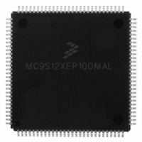
MC9S12XEP100MAL Freescale Semiconductor, MC9S12XEP100MAL Datasheet - Page 169

MC9S12XEP100MAL
Manufacturer Part Number
MC9S12XEP100MAL
Description
IC MCU 16BIT 1M FLASH 112-LQFP
Manufacturer
Freescale Semiconductor
Series
HCS12r
Datasheet
1.MC9S12XEP768CAL.pdf
(1328 pages)
Specifications of MC9S12XEP100MAL
Core Processor
HCS12X
Core Size
16-Bit
Speed
50MHz
Connectivity
CAN, EBI/EMI, I²C, IrDA, SCI, SPI
Peripherals
LVD, POR, PWM, WDT
Number Of I /o
91
Program Memory Size
1MB (1M x 8)
Program Memory Type
FLASH
Eeprom Size
4K x 8
Ram Size
64K x 8
Voltage - Supply (vcc/vdd)
1.72 V ~ 5.5 V
Data Converters
A/D 16x12b
Oscillator Type
External
Operating Temperature
-40°C ~ 125°C
Package / Case
112-LQFP
Processor Series
S12XE
Core
HCS12
Data Bus Width
16 bit
Data Ram Size
64 KB
Interface Type
SPI, SSI
Maximum Clock Frequency
50 MHz
Number Of Programmable I/os
91
Number Of Timers
25
Operating Supply Voltage
- 0.3 V to + 6 V
Maximum Operating Temperature
+ 105 C
Mounting Style
SMD/SMT
3rd Party Development Tools
EWHCS12
Development Tools By Supplier
KIT33812ECUEVME, EVB9S12XEP100, DEMO9S12XEP100
Minimum Operating Temperature
- 40 C
On-chip Adc
10 bit, 16 Channel
For Use With
EVB9S12XEP100 - BOARD EVAL FOR MC9S12XEP100DEMO9S12XEP100 - BOARD DEMO FOR MC9S12XEP100
Lead Free Status / RoHS Status
Lead free / RoHS Compliant
Available stocks
Company
Part Number
Manufacturer
Quantity
Price
Company:
Part Number:
MC9S12XEP100MAL
Manufacturer:
Freescale Semiconductor
Quantity:
10 000
Part Number:
MC9S12XEP100MAL
Manufacturer:
FREESCALE
Quantity:
20 000
- Current page: 169 of 1328
- Download datasheet (9Mb)
1. Read: Anytime.
1. Read: Anytime.
2.3.87
2.3.88
Freescale Semiconductor
Address 0x036A
Address 0x036B
Write: Anytime.
Write: Anytime.
DDRR
Field
Reset
Reset
7-0
W
W
R
R
Port R data direction—
This register controls the data direction of pins 7 through 0.
The TIM forces the I/O state to be an output for each timer port associated with an enabled output compare. In this
case the data direction bits will not change.
The data direction bits revert to controlling the I/O direction of a pin when the associated timer output compare is
disabled.
The timer Input Capture always monitors the state of the pin.
1 Associated pin is configured as output.
0 Associated pin is configured as high-impedance input.
DDRR7
RDRR7
Port R Data Direction Register (DDRR)
Port R Reduced Drive Register (RDRR)
0
0
7
7
Due to internal synchronization circuits, it can take up to 2 bus clock cycles
until the correct value is read on PTR or PTIR registers, when changing the
DDRR register.
DDRR6
RDRR6
0
0
6
6
Figure 2-86. Port R Reduced Drive Register (RDRR)
Figure 2-85. Port R Data Direction Register (DDRR)
Table 2-83. DDRR Register Field Descriptions
MC9S12XE-Family Reference Manual , Rev. 1.23
DDRR5
RDRR5
0
0
5
5
DDRR4
RDRR4
NOTE
0
0
4
4
Description
DDRR3
RDRR3
3
0
3
0
Chapter 2 Port Integration Module (S12XEPIMV1)
DDRR2
RDRR2
0
0
2
2
Access: User read/write
Access: User read/write
DDRR1
RDRR1
0
0
1
1
DDRR0
RDRR0
0
0
0
0
169
(1)
(1)
Related parts for MC9S12XEP100MAL
Image
Part Number
Description
Manufacturer
Datasheet
Request
R
Part Number:
Description:
Manufacturer:
Freescale Semiconductor, Inc
Datasheet:
Part Number:
Description:
Manufacturer:
Freescale Semiconductor, Inc
Datasheet:
Part Number:
Description:
Manufacturer:
Freescale Semiconductor, Inc
Datasheet:
Part Number:
Description:
Manufacturer:
Freescale Semiconductor, Inc
Datasheet:
Part Number:
Description:
Manufacturer:
Freescale Semiconductor, Inc
Datasheet:
Part Number:
Description:
Manufacturer:
Freescale Semiconductor, Inc
Datasheet:
Part Number:
Description:
Manufacturer:
Freescale Semiconductor, Inc
Datasheet:
Part Number:
Description:
Manufacturer:
Freescale Semiconductor, Inc
Datasheet:
Part Number:
Description:
Manufacturer:
Freescale Semiconductor, Inc
Datasheet:
Part Number:
Description:
Manufacturer:
Freescale Semiconductor, Inc
Datasheet:
Part Number:
Description:
Manufacturer:
Freescale Semiconductor, Inc
Datasheet:
Part Number:
Description:
Manufacturer:
Freescale Semiconductor, Inc
Datasheet:
Part Number:
Description:
Manufacturer:
Freescale Semiconductor, Inc
Datasheet:
Part Number:
Description:
Manufacturer:
Freescale Semiconductor, Inc
Datasheet:
Part Number:
Description:
Manufacturer:
Freescale Semiconductor, Inc
Datasheet:


