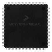
MC9S12XEP100MAL Freescale Semiconductor, MC9S12XEP100MAL Datasheet - Page 781

MC9S12XEP100MAL
Manufacturer Part Number
MC9S12XEP100MAL
Description
IC MCU 16BIT 1M FLASH 112-LQFP
Manufacturer
Freescale Semiconductor
Series
HCS12r
Datasheet
1.MC9S12XEP768CAL.pdf
(1328 pages)
Specifications of MC9S12XEP100MAL
Core Processor
HCS12X
Core Size
16-Bit
Speed
50MHz
Connectivity
CAN, EBI/EMI, I²C, IrDA, SCI, SPI
Peripherals
LVD, POR, PWM, WDT
Number Of I /o
91
Program Memory Size
1MB (1M x 8)
Program Memory Type
FLASH
Eeprom Size
4K x 8
Ram Size
64K x 8
Voltage - Supply (vcc/vdd)
1.72 V ~ 5.5 V
Data Converters
A/D 16x12b
Oscillator Type
External
Operating Temperature
-40°C ~ 125°C
Package / Case
112-LQFP
Processor Series
S12XE
Core
HCS12
Data Bus Width
16 bit
Data Ram Size
64 KB
Interface Type
SPI, SSI
Maximum Clock Frequency
50 MHz
Number Of Programmable I/os
91
Number Of Timers
25
Operating Supply Voltage
- 0.3 V to + 6 V
Maximum Operating Temperature
+ 105 C
Mounting Style
SMD/SMT
3rd Party Development Tools
EWHCS12
Development Tools By Supplier
KIT33812ECUEVME, EVB9S12XEP100, DEMO9S12XEP100
Minimum Operating Temperature
- 40 C
On-chip Adc
10 bit, 16 Channel
For Use With
EVB9S12XEP100 - BOARD EVAL FOR MC9S12XEP100DEMO9S12XEP100 - BOARD DEMO FOR MC9S12XEP100
Lead Free Status / RoHS Status
Lead free / RoHS Compliant
Available stocks
Company
Part Number
Manufacturer
Quantity
Price
Company:
Part Number:
MC9S12XEP100MAL
Manufacturer:
Freescale Semiconductor
Quantity:
10 000
Part Number:
MC9S12XEP100MAL
Manufacturer:
FREESCALE
Quantity:
20 000
- Current page: 781 of 1328
- Download datasheet (9Mb)
In slave mode, if the SS line is not deasserted between the successive transmissions then the content of the
SPI data register is not transmitted; instead the last received data is transmitted. If the SS line is deasserted
for at least minimum idle time (half SCK cycle) between successive transmissions, then the content of the
SPI data register is transmitted.
In master mode, with slave select output enabled the SS line is always deasserted and reasserted between
successive transfers for at least minimum idle time.
21.4.3.3
Some peripherals require the first SCK edge before the first data bit becomes available at the data out pin,
the second edge clocks data into the system. In this format, the first SCK edge is issued by setting the
CPHA bit at the beginning of the n
The first edge of SCK occurs immediately after the half SCK clock cycle synchronization delay. This first
edge commands the slave to transfer its first data bit to the serial data input pin of the master.
A half SCK cycle later, the second edge appears on the SCK pin. This is the latching edge for both the
master and slave.
1. n depends on the selected transfer width, please refer to
Freescale Semiconductor
Because of an order from the United States International Trade Commission, BGA-packaged product lines and partnumbers
indicated here currently are not available from Freescale for import or sale in the United States prior to September 2010
End of Idle State
SCK Edge Number
SCK (CPOL = 0)
SCK (CPOL = 1)
SAMPLE I
MOSI/MISO
CHANGE O
CHANGE O
SEL SS (O)
Master only
SEL SS (I)
t
t
t
t
Figure 21-13. SPI Clock Format 0 (CPHA = 0), with 16-Bit Transfer Width selected (XFRW = 1)
MOSI pin
MISO pin
L
T
I
L
MSB first (LSBFE = 0)
, t
LSB first (LSBFE = 1)
= Minimum idling time between transfers (minimum SS high time)
= Minimum leading time before the first SCK edge
= Minimum trailing time after the last SCK edge
T
, and t
CPHA = 1 Transfer Format
I
are guaranteed for the master mode and required for the slave mode.
MSB
LSB
t
L
1
2
Bit 14
Bit 1
3
4
Bit 13
Bit 2
MC9S12XE-Family Reference Manual Rev. 1.23
5
Begin
6
1
Bit 12
Bit 3
-cycle transfer operation.
7
8
Bit 11
Bit 4
9
10
Bit 10 Bit 9 Bit 8 Bit 7 Bit 6
Bit 5
11
12
Bit 6
13
14
Section 21.3.2.2, “SPI Control Register 2 (SPICR2)
Transfer
Bit 7 Bit 8 Bit 9 Bit 10Bit 11Bit 12Bit 13Bit 14
15
16
17
18
19
20
Bit 5
21
22
Bit 4 Bit 3 Bit 2 Bit 1
23
Chapter 21 Serial Peripheral Interface (S12SPIV5)
24
25
End
26
27
28
29
30
MSB
LSB
31
32
t
T
Minimum 1/2 SCK
for t
Begin of Idle State
t
I
t
T
L
, t
l
, t
L
781
Related parts for MC9S12XEP100MAL
Image
Part Number
Description
Manufacturer
Datasheet
Request
R
Part Number:
Description:
Manufacturer:
Freescale Semiconductor, Inc
Datasheet:
Part Number:
Description:
Manufacturer:
Freescale Semiconductor, Inc
Datasheet:
Part Number:
Description:
Manufacturer:
Freescale Semiconductor, Inc
Datasheet:
Part Number:
Description:
Manufacturer:
Freescale Semiconductor, Inc
Datasheet:
Part Number:
Description:
Manufacturer:
Freescale Semiconductor, Inc
Datasheet:
Part Number:
Description:
Manufacturer:
Freescale Semiconductor, Inc
Datasheet:
Part Number:
Description:
Manufacturer:
Freescale Semiconductor, Inc
Datasheet:
Part Number:
Description:
Manufacturer:
Freescale Semiconductor, Inc
Datasheet:
Part Number:
Description:
Manufacturer:
Freescale Semiconductor, Inc
Datasheet:
Part Number:
Description:
Manufacturer:
Freescale Semiconductor, Inc
Datasheet:
Part Number:
Description:
Manufacturer:
Freescale Semiconductor, Inc
Datasheet:
Part Number:
Description:
Manufacturer:
Freescale Semiconductor, Inc
Datasheet:
Part Number:
Description:
Manufacturer:
Freescale Semiconductor, Inc
Datasheet:
Part Number:
Description:
Manufacturer:
Freescale Semiconductor, Inc
Datasheet:
Part Number:
Description:
Manufacturer:
Freescale Semiconductor, Inc
Datasheet:


