MC9S12XEP100MAL Freescale Semiconductor, MC9S12XEP100MAL Datasheet - Page 728
MC9S12XEP100MAL
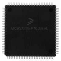
Manufacturer Part Number
MC9S12XEP100MAL
Description
IC MCU 16BIT 1M FLASH 112-LQFP
Manufacturer
Freescale Semiconductor
Series
HCS12r
Datasheet
1.MC9S12XEP768CAL.pdf
(1328 pages)
Specifications of MC9S12XEP100MAL
Core Processor
HCS12X
Core Size
16-Bit
Speed
50MHz
Connectivity
CAN, EBI/EMI, I²C, IrDA, SCI, SPI
Peripherals
LVD, POR, PWM, WDT
Number Of I /o
91
Program Memory Size
1MB (1M x 8)
Program Memory Type
FLASH
Eeprom Size
4K x 8
Ram Size
64K x 8
Voltage - Supply (vcc/vdd)
1.72 V ~ 5.5 V
Data Converters
A/D 16x12b
Oscillator Type
External
Operating Temperature
-40°C ~ 125°C
Package / Case
112-LQFP
Processor Series
S12XE
Core
HCS12
Data Bus Width
16 bit
Data Ram Size
64 KB
Interface Type
SPI, SSI
Maximum Clock Frequency
50 MHz
Number Of Programmable I/os
91
Number Of Timers
25
Operating Supply Voltage
- 0.3 V to + 6 V
Maximum Operating Temperature
+ 105 C
Mounting Style
SMD/SMT
3rd Party Development Tools
EWHCS12
Development Tools By Supplier
KIT33812ECUEVME, EVB9S12XEP100, DEMO9S12XEP100
Minimum Operating Temperature
- 40 C
On-chip Adc
10 bit, 16 Channel
For Use With
EVB9S12XEP100 - BOARD EVAL FOR MC9S12XEP100DEMO9S12XEP100 - BOARD DEMO FOR MC9S12XEP100
Lead Free Status / RoHS Status
Lead free / RoHS Compliant
Available stocks
Company
Part Number
Manufacturer
Quantity
Price

Company:
Part Number:
MC9S12XEP100MAL
Manufacturer:
Freescale Semiconductor
Quantity:
10 000
Part Number:
MC9S12XEP100MAL
Manufacturer:
FREESCALE
Quantity:
20 000


Chapter 20 Serial Communication Interface (S12SCIV5)
20.2
The SCI module has a total of two external pins.
20.2.1
The TXD pin transmits SCI (standard or infrared) data. It will idle high in either mode and is high
impedance anytime the transmitter is disabled.
20.2.2
The RXD pin receives SCI (standard or infrared) data. An idle line is detected as a line high. This input is
ignored when the receiver is disabled and should be terminated to a known voltage.
20.3
This section provides a detailed description of all the SCI registers.
20.3.1
The memory map for the SCI module is given below in
the address offset. The total address for each register is the sum of the base address for the SCI module and
the address offset for each register.
728
Because of an order from the United States International Trade Commission, BGA-packaged product lines and partnumbers
indicated here currently are not available from Freescale for import or sale in the United States prior to September 2010
External Signal Description
Memory Map and Register Definition
TXD — Transmit Pin
RXD — Receive Pin
Module Memory Map and Register Definition
MC9S12XE-Family Reference Manual , Rev. 1.23
Figure
20-2. The address listed for each register is
Freescale Semiconductor
Related parts for MC9S12XEP100MAL
Image
Part Number
Description
Manufacturer
Datasheet
Request
R

Part Number:
Description:
Manufacturer:
Freescale Semiconductor, Inc
Datasheet:
Part Number:
Description:
Manufacturer:
Freescale Semiconductor, Inc
Datasheet:
Part Number:
Description:
Manufacturer:
Freescale Semiconductor, Inc
Datasheet:
Part Number:
Description:
Manufacturer:
Freescale Semiconductor, Inc
Datasheet:
Part Number:
Description:
Manufacturer:
Freescale Semiconductor, Inc
Datasheet:
Part Number:
Description:
Manufacturer:
Freescale Semiconductor, Inc
Datasheet:
Part Number:
Description:
Manufacturer:
Freescale Semiconductor, Inc
Datasheet:
Part Number:
Description:
Manufacturer:
Freescale Semiconductor, Inc
Datasheet:
Part Number:
Description:
Manufacturer:
Freescale Semiconductor, Inc
Datasheet:
Part Number:
Description:
Manufacturer:
Freescale Semiconductor, Inc
Datasheet:
Part Number:
Description:
Manufacturer:
Freescale Semiconductor, Inc
Datasheet:
Part Number:
Description:
Manufacturer:
Freescale Semiconductor, Inc
Datasheet:
Part Number:
Description:
Manufacturer:
Freescale Semiconductor, Inc
Datasheet:
Part Number:
Description:
Manufacturer:
Freescale Semiconductor, Inc
Datasheet:
Part Number:
Description:
Manufacturer:
Freescale Semiconductor, Inc
Datasheet: