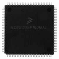
MC9S12XEP100MAL Freescale Semiconductor, MC9S12XEP100MAL Datasheet - Page 63

MC9S12XEP100MAL
Manufacturer Part Number
MC9S12XEP100MAL
Description
IC MCU 16BIT 1M FLASH 112-LQFP
Manufacturer
Freescale Semiconductor
Series
HCS12r
Datasheet
1.MC9S12XEP768CAL.pdf
(1328 pages)
Specifications of MC9S12XEP100MAL
Core Processor
HCS12X
Core Size
16-Bit
Speed
50MHz
Connectivity
CAN, EBI/EMI, I²C, IrDA, SCI, SPI
Peripherals
LVD, POR, PWM, WDT
Number Of I /o
91
Program Memory Size
1MB (1M x 8)
Program Memory Type
FLASH
Eeprom Size
4K x 8
Ram Size
64K x 8
Voltage - Supply (vcc/vdd)
1.72 V ~ 5.5 V
Data Converters
A/D 16x12b
Oscillator Type
External
Operating Temperature
-40°C ~ 125°C
Package / Case
112-LQFP
Processor Series
S12XE
Core
HCS12
Data Bus Width
16 bit
Data Ram Size
64 KB
Interface Type
SPI, SSI
Maximum Clock Frequency
50 MHz
Number Of Programmable I/os
91
Number Of Timers
25
Operating Supply Voltage
- 0.3 V to + 6 V
Maximum Operating Temperature
+ 105 C
Mounting Style
SMD/SMT
3rd Party Development Tools
EWHCS12
Development Tools By Supplier
KIT33812ECUEVME, EVB9S12XEP100, DEMO9S12XEP100
Minimum Operating Temperature
- 40 C
On-chip Adc
10 bit, 16 Channel
For Use With
EVB9S12XEP100 - BOARD EVAL FOR MC9S12XEP100DEMO9S12XEP100 - BOARD DEMO FOR MC9S12XEP100
Lead Free Status / RoHS Status
Lead free / RoHS Compliant
Available stocks
Company
Part Number
Manufacturer
Quantity
Price
Company:
Part Number:
MC9S12XEP100MAL
Manufacturer:
Freescale Semiconductor
Quantity:
10 000
Part Number:
MC9S12XEP100MAL
Manufacturer:
FREESCALE
Quantity:
20 000
- Current page: 63 of 1328
- Download datasheet (9Mb)
1.2.3.7
PA[7:0] are general-purpose input or output pins. In MCU expanded modes of operation, these pins are
used for the external address bus. In MCU emulation modes of operation, these pins are used for external
address bus and internal visibility read data.
1.2.3.8
PB[7:1] are general-purpose input or output pins. In MCU expanded modes of operation, these pins are
used for the external address bus. In MCU emulation modes of operation, these pins are used for external
address bus and internal visibility read data.
1.2.3.9
PB0 is a general-purpose input or output pin. In MCU expanded modes of operation, this pin is used for
the external address bus ADDR0 or as upper data strobe signal. In MCU emulation modes of operation,
this pin is used for external address bus ADDR0 and internal visibility read data IVD0.
1.2.3.10
PC[7:0] are general-purpose input or output pins. In MCU expanded modes of operation, these pins are
used for the external data bus.
The input voltage thresholds for PC[7:0] can be configured to reduced levels, to allow data from an external
3.3-V peripheral to be read by the MCU operating at 5.0 V. The input voltage thresholds for PC[7:0] are
configured to reduced levels out of reset in expanded and emulation modes. The input voltage thresholds
for PC[7:0] are configured to 5-V levels out of reset in normal modes.
1.2.3.11
PD[7:0] are general-purpose input or output pins. In MCU expanded modes of operation, these pins are
used for the external data bus.
The input voltage thresholds for PD[7:0] can be configured to reduced levels, to allow data from an
external 3.3-V peripheral to be read by the MCU operating at 5.0 V. The input voltage thresholds for
PD[7:0] are configured to reduced levels out of reset in expanded and emulation modes. The input voltage
thresholds for PC[7:0] are configured to 5-V levels out of reset in normal modes.
1.2.3.12
PE7 is a general-purpose input or output pin. ECLKX2 is a free running clock of twice the internal bus
frequency, available by default in emulation modes and when enabled in other modes. The XCLKS is an
input signal which controls whether a crystal in combination with the internal loop controlled Pierce
oscillator is used or whether full swing Pierce oscillator/external clock circuitry is used (refer to
Configuration). An internal pullup is enabled during reset.
Freescale Semiconductor
Because of an order from the United States International Trade Commission, BGA-packaged product lines and partnumbers
indicated here currently are not available from Freescale for import or sale in the United States prior to September 2010
PA[7:0] / ADDR[15:8] / IVD[15:8] — Port A I/O Pins
PB[7:1] / ADDR[7:1] / IVD[7:1] — Port B I/O Pins
PB0 / ADDR0 / UDS / IVD[0] — Port B I/O Pin 0
PC[7:0] / DATA [15:8] — Port C I/O Pins
PD[7:0] / DATA [7:0] — Port D I/O Pins
PE7 / ECLKX2 / XCLKS — Port E I/O Pin 7
MC9S12XE-Family Reference Manual Rev. 1.23
Chapter 1 Device Overview MC9S12XE-Family
Oscillator
63
Related parts for MC9S12XEP100MAL
Image
Part Number
Description
Manufacturer
Datasheet
Request
R
Part Number:
Description:
Manufacturer:
Freescale Semiconductor, Inc
Datasheet:
Part Number:
Description:
Manufacturer:
Freescale Semiconductor, Inc
Datasheet:
Part Number:
Description:
Manufacturer:
Freescale Semiconductor, Inc
Datasheet:
Part Number:
Description:
Manufacturer:
Freescale Semiconductor, Inc
Datasheet:
Part Number:
Description:
Manufacturer:
Freescale Semiconductor, Inc
Datasheet:
Part Number:
Description:
Manufacturer:
Freescale Semiconductor, Inc
Datasheet:
Part Number:
Description:
Manufacturer:
Freescale Semiconductor, Inc
Datasheet:
Part Number:
Description:
Manufacturer:
Freescale Semiconductor, Inc
Datasheet:
Part Number:
Description:
Manufacturer:
Freescale Semiconductor, Inc
Datasheet:
Part Number:
Description:
Manufacturer:
Freescale Semiconductor, Inc
Datasheet:
Part Number:
Description:
Manufacturer:
Freescale Semiconductor, Inc
Datasheet:
Part Number:
Description:
Manufacturer:
Freescale Semiconductor, Inc
Datasheet:
Part Number:
Description:
Manufacturer:
Freescale Semiconductor, Inc
Datasheet:
Part Number:
Description:
Manufacturer:
Freescale Semiconductor, Inc
Datasheet:
Part Number:
Description:
Manufacturer:
Freescale Semiconductor, Inc
Datasheet:


