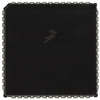
MC68HC711E9CFNE2 Freescale Semiconductor, MC68HC711E9CFNE2 Datasheet - Page 244

MC68HC711E9CFNE2
Manufacturer Part Number
MC68HC711E9CFNE2
Description
IC MCU 8BIT 512RAM 52-PLC
Manufacturer
Freescale Semiconductor
Series
HC11r
Datasheet
1.MC68HC711E9CFNE3.pdf
(336 pages)
Specifications of MC68HC711E9CFNE2
Core Processor
HC11
Core Size
8-Bit
Speed
2MHz
Connectivity
SCI, SPI
Peripherals
POR, WDT
Number Of I /o
38
Program Memory Size
12KB (12K x 8)
Program Memory Type
OTP
Eeprom Size
512 x 8
Ram Size
512 x 8
Voltage - Supply (vcc/vdd)
4.5 V ~ 5.5 V
Data Converters
A/D 8x8b
Oscillator Type
Internal
Operating Temperature
-40°C ~ 85°C
Package / Case
52-PLCC
Processor Series
HC711E
Core
HC11
Data Bus Width
8 bit
Data Ram Size
512 B
Interface Type
SCI, SPI
Maximum Clock Frequency
2 MHz
Number Of Programmable I/os
38
Number Of Timers
8
Maximum Operating Temperature
+ 85 C
Mounting Style
SMD/SMT
Minimum Operating Temperature
- 40 C
On-chip Adc
8 bit
Lead Free Status / RoHS Status
Lead free / RoHS Compliant
Available stocks
Company
Part Number
Manufacturer
Quantity
Price
Company:
Part Number:
MC68HC711E9CFNE2
Manufacturer:
TE
Quantity:
12 000
Company:
Part Number:
MC68HC711E9CFNE2
Manufacturer:
FREESCAL
Quantity:
5 530
- Current page: 244 of 336
- Download datasheet (4Mb)
Electrical Characteristics
11.17 MC68L11E9 Expansion Bus Timing Characteristics
Technical Data
244
Num
1. V
2. Input clocks with duty cycles other than 50% affect bus performance. Timing parameters affected by input clock duty cycle
4a
4b
12
17
18
19
21
22
24
25
26
27
28
29
35
36
1
2
3
9
otherwise noted
are identified by (a) and (b). To recalculate the approximate bus timing values, substitute the following expressions in place
of 1/8 t
DD
Where:
Frequency of operation (E-clock frequency)
Cycle time
Pulse width, E low, PW
Pulse width, E high, PW
E and AS rise time
E and AS fall time
Address hold time
Non-multiplexed address valid time to E rise
Read data setup time
Read data hold time , max = t
Write data delay time, t
Write data hold time, t
Multiplexed address valid time to E rise
Multiplexed address valid time to AS fall
Multiplexed address hold time, t
Delay time, E to AS rise, t
Pulse width, AS high, PW
Delay time, AS to E rise, t
MPU address access time
MPU access time, t
Multiplexed address delay (Previous cycle MPU read)
= 3.0 Vdc to 5.5 Vdc, V
(a) (1–dc)
(b) dc
dc is the decimal value of duty cycle percentage (high time).
t
t
t
t
AV
AVM
ASL
ACCA
cyc
t
MAD
= PW
in the above formulas, where applicable:
= PW
= PW
= t
= t
1/4 t
cyc
EL
ASD
ASH
EL
1/4 t
cyc
–(t
–(PW
–(t
+ 30 ns
–70 ns
ASD
cyc
ASD
(2) (2)a
EL
ACCE
+ 80 ns)
Characteristic
–t
SS
DHW
+ 90 ns)
DDW
(2)a
EL
AVM
EH
, t
= 0 Vdc, T
= PW
ASH
ASD
ASED
AH
= 1/2 t
(3)a
= 1/8 t
= 1/2 t
) –t
= 1/8 t
(2)a
= 1/8 t
MAD
= 1/4 t
= 1/8 t
(2)a
DSR
EH
= 1/8 t
AHL
cyc
cyc
cyc
A
–t
cyc
–t
= T
cyc
–25 ns
DSR
(1)
= 1/8 t
cyc
f
–30 ns
cyc
–30 ns
Electrical Characteristics
+ 70 ns
cyc
L
–30 ns
–30 ns
–5 ns
to T
–5 ns
cyc
(2)a
H
, all timing is shown with respect to 20% V
(2)a
(2)a
–30 ns
(2)b
(2)b
Symbol
PW
PW
PW
t
t
t
t
t
t
t
t
t
ACCA
ACCE
t
t
ASED
t
DDW
DHW
t
DHR
MAD
t
DSR
AVM
ASD
t
ASL
AHL
cyc
AH
f
AV
t
t
o
r
ASH
f
EH
EL
1000
Min
475
470
275
268
150
120
220
120
735
150
dc
95
30
95
95
—
—
—
—
0
1.0 MHz
M68HC11E Family — Rev. 3.2
Max
150
195
440
1.0
—
—
—
25
25
—
—
—
—
—
—
—
—
—
—
—
—
DD
and 70% V
Min
500
225
220
298
dc
33
88
30
33
78
25
33
58
95
58
88
—
—
—
—
0
2.0 MHz
MOTOROLA
Max
133
190
2.0
DD
25
25
88
—
—
—
—
—
—
—
—
—
—
—
—
—
—
—
, unless
MHz
Unit
ns
ns
ns
ns
ns
ns
ns
ns
ns
ns
ns
ns
ns
ns
ns
ns
ns
ns
ns
ns
Related parts for MC68HC711E9CFNE2
Image
Part Number
Description
Manufacturer
Datasheet
Request
R

Part Number:
Description:
APPENDIX A ELECTRICAL CHARACTERISTICS
Manufacturer:
FREESCALE [Freescale Semiconductor, Inc]
Datasheet:
Part Number:
Description:
Manufacturer:
Freescale Semiconductor, Inc
Datasheet:
Part Number:
Description:
Manufacturer:
Freescale Semiconductor, Inc
Datasheet:
Part Number:
Description:
Manufacturer:
Freescale Semiconductor, Inc
Datasheet:
Part Number:
Description:
Manufacturer:
Freescale Semiconductor, Inc
Datasheet:
Part Number:
Description:
Manufacturer:
Freescale Semiconductor, Inc
Datasheet:
Part Number:
Description:
Manufacturer:
Freescale Semiconductor, Inc
Datasheet:
Part Number:
Description:
Manufacturer:
Freescale Semiconductor, Inc
Datasheet:
Part Number:
Description:
Manufacturer:
Freescale Semiconductor, Inc
Datasheet:
Part Number:
Description:
Manufacturer:
Freescale Semiconductor, Inc
Datasheet:
Part Number:
Description:
Manufacturer:
Freescale Semiconductor, Inc
Datasheet:
Part Number:
Description:
Manufacturer:
Freescale Semiconductor, Inc
Datasheet:
Part Number:
Description:
Manufacturer:
Freescale Semiconductor, Inc
Datasheet:
Part Number:
Description:
Manufacturer:
Freescale Semiconductor, Inc
Datasheet:
Part Number:
Description:
Manufacturer:
Freescale Semiconductor, Inc
Datasheet:


