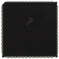
MC68HC711E9CFNE2 Freescale Semiconductor, MC68HC711E9CFNE2 Datasheet - Page 312

MC68HC711E9CFNE2
Manufacturer Part Number
MC68HC711E9CFNE2
Description
IC MCU 8BIT 512RAM 52-PLC
Manufacturer
Freescale Semiconductor
Series
HC11r
Datasheet
1.MC68HC711E9CFNE3.pdf
(336 pages)
Specifications of MC68HC711E9CFNE2
Core Processor
HC11
Core Size
8-Bit
Speed
2MHz
Connectivity
SCI, SPI
Peripherals
POR, WDT
Number Of I /o
38
Program Memory Size
12KB (12K x 8)
Program Memory Type
OTP
Eeprom Size
512 x 8
Ram Size
512 x 8
Voltage - Supply (vcc/vdd)
4.5 V ~ 5.5 V
Data Converters
A/D 8x8b
Oscillator Type
Internal
Operating Temperature
-40°C ~ 85°C
Package / Case
52-PLCC
Processor Series
HC711E
Core
HC11
Data Bus Width
8 bit
Data Ram Size
512 B
Interface Type
SCI, SPI
Maximum Clock Frequency
2 MHz
Number Of Programmable I/os
38
Number Of Timers
8
Maximum Operating Temperature
+ 85 C
Mounting Style
SMD/SMT
Minimum Operating Temperature
- 40 C
On-chip Adc
8 bit
Lead Free Status / RoHS Status
Lead free / RoHS Compliant
Available stocks
Company
Part Number
Manufacturer
Quantity
Price
Company:
Part Number:
MC68HC711E9CFNE2
Manufacturer:
TE
Quantity:
12 000
Company:
Part Number:
MC68HC711E9CFNE2
Manufacturer:
FREESCAL
Quantity:
5 530
- Current page: 312 of 336
- Download datasheet (4Mb)
Application Note
Connecting RxD
to V
Cause the SCI
to Receive a Break
$FF Character Is
Required before
Loading into RAM
312
SS
Does Not
Between these times, the bootloader program is executed, which
changes the states of some systems and control bits:
Users also forget that bootstrap mode is a special mode. Thus,
privileged control bits are accessible, and write protection for some
registers is not in effect. The bootstrap ROM is in the memory map. The
DISR bit in the TEST1 control register is set, which disables resets from
the COP and clock monitor systems.
Since bootstrap is a special mode, these conditions can be changed by
software. The bus can even be switched from single-chip mode to
expanded mode to gain access to external memories and peripherals.
To force an immediate jump to the start of EEPROM, the bootstrap
firmware looks for the first received character to be $00 (or break). The
data reception logic in the SCI looks for a 1-to-0 transition on the RxD
pin to synchronize to the beginning of a receive character. If the RxD pin
is tied to ground, no 1-to-0 transition occurs. The SCI transmitter sends
a break character when the bootloader firmware starts, and this break
character can be fed back to the RxD pin to cause the jump to EEPROM.
Since TxD is configured as an open-drain output, a pullup resistor is
required.
The initial character (usually $FF) that sets the download baud rate is
often forgotten.
•
•
•
•
•
•
The SCI system is initialized and turned on (Rx and Tx).
The SCI system has control of the PD0 and PD1 pins.
Port D outputs are configured for wire-OR operation.
The stack pointer is initialized to the top of RAM.
Time has passed (two or more SCI character times).
Timer has advanced from its reset count value.
AN1060 — Rev. 1.0
MOTOROLA
Related parts for MC68HC711E9CFNE2
Image
Part Number
Description
Manufacturer
Datasheet
Request
R

Part Number:
Description:
APPENDIX A ELECTRICAL CHARACTERISTICS
Manufacturer:
FREESCALE [Freescale Semiconductor, Inc]
Datasheet:
Part Number:
Description:
Manufacturer:
Freescale Semiconductor, Inc
Datasheet:
Part Number:
Description:
Manufacturer:
Freescale Semiconductor, Inc
Datasheet:
Part Number:
Description:
Manufacturer:
Freescale Semiconductor, Inc
Datasheet:
Part Number:
Description:
Manufacturer:
Freescale Semiconductor, Inc
Datasheet:
Part Number:
Description:
Manufacturer:
Freescale Semiconductor, Inc
Datasheet:
Part Number:
Description:
Manufacturer:
Freescale Semiconductor, Inc
Datasheet:
Part Number:
Description:
Manufacturer:
Freescale Semiconductor, Inc
Datasheet:
Part Number:
Description:
Manufacturer:
Freescale Semiconductor, Inc
Datasheet:
Part Number:
Description:
Manufacturer:
Freescale Semiconductor, Inc
Datasheet:
Part Number:
Description:
Manufacturer:
Freescale Semiconductor, Inc
Datasheet:
Part Number:
Description:
Manufacturer:
Freescale Semiconductor, Inc
Datasheet:
Part Number:
Description:
Manufacturer:
Freescale Semiconductor, Inc
Datasheet:
Part Number:
Description:
Manufacturer:
Freescale Semiconductor, Inc
Datasheet:
Part Number:
Description:
Manufacturer:
Freescale Semiconductor, Inc
Datasheet:


