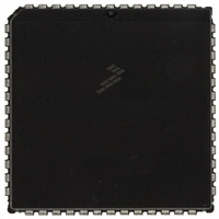
MC68HC711E9CFNE2 Freescale Semiconductor, MC68HC711E9CFNE2 Datasheet - Page 98

MC68HC711E9CFNE2
Manufacturer Part Number
MC68HC711E9CFNE2
Description
IC MCU 8BIT 512RAM 52-PLC
Manufacturer
Freescale Semiconductor
Series
HC11r
Datasheet
1.MC68HC711E9CFNE3.pdf
(336 pages)
Specifications of MC68HC711E9CFNE2
Core Processor
HC11
Core Size
8-Bit
Speed
2MHz
Connectivity
SCI, SPI
Peripherals
POR, WDT
Number Of I /o
38
Program Memory Size
12KB (12K x 8)
Program Memory Type
OTP
Eeprom Size
512 x 8
Ram Size
512 x 8
Voltage - Supply (vcc/vdd)
4.5 V ~ 5.5 V
Data Converters
A/D 8x8b
Oscillator Type
Internal
Operating Temperature
-40°C ~ 85°C
Package / Case
52-PLCC
Processor Series
HC711E
Core
HC11
Data Bus Width
8 bit
Data Ram Size
512 B
Interface Type
SCI, SPI
Maximum Clock Frequency
2 MHz
Number Of Programmable I/os
38
Number Of Timers
8
Maximum Operating Temperature
+ 85 C
Mounting Style
SMD/SMT
Minimum Operating Temperature
- 40 C
On-chip Adc
8 bit
Lead Free Status / RoHS Status
Lead free / RoHS Compliant
Available stocks
Company
Part Number
Manufacturer
Quantity
Price
Company:
Part Number:
MC68HC711E9CFNE2
Manufacturer:
TE
Quantity:
12 000
Company:
Part Number:
MC68HC711E9CFNE2
Manufacturer:
FREESCAL
Quantity:
5 530
- Current page: 98 of 336
- Download datasheet (4Mb)
Operating Modes and On-Chip Memory
4.6 EEPROM
4.6.1 EEPROM and CONFIG Programming and Erasure
Technical Data
98
PGM — EPROM Programming Voltage Enable Bit
Some E-series devices contain 512 bytes of on-chip EEPROM. The
MC68HC811E2 contains 2048 bytes of EEPROM with selectable base
address. All E-series devices contain the EEPROM-based CONFIG
register.
The erased state of an EEPROM bit is 1. During a read operation, bit
lines are precharged to 1. The floating gate devices of programmed bits
conduct and pull the bit lines to 0. Unprogrammed bits remain at the
precharged level and are read as 1s. Programming a bit to 1 causes no
change. Programming a bit to 0 changes the bit so that subsequent
reads return 0.
When appropriate bits in the BPROT register are cleared, the PPROG
register controls programming and erasing the EEPROM. The PPROG
register can be read or written at any time, but logic enforces defined
programming and erasing sequences to prevent unintentional changes
to EEPROM data. When the EELAT bit in the PPROG register is cleared,
the EEPROM can be read as if it were a ROM.
The on-chip charge pump that generates the EEPROM programming
voltage from V
value. The efficiency of this charge pump and its drive capability are
affected by the level of V
load depends on the number of bits being programmed or erased and
capacitances in the EEPROM array.
The clock source driving the charge pump is software selectable. When
the clock select (CSEL) bit in the OPTION register is 0, the E clock is
PGM can be read any time and can be written only when ELAT = 1.
0 = Programming voltage to EPROM array disconnected
1 = Programming voltage to EPROM array connected
Operating Modes and On-Chip Memory
DD
uses MOS capacitors, which are relatively small in
DD
and the frequency of the driving clock. The
M68HC11E Family — Rev. 3.2
MOTOROLA
Related parts for MC68HC711E9CFNE2
Image
Part Number
Description
Manufacturer
Datasheet
Request
R

Part Number:
Description:
APPENDIX A ELECTRICAL CHARACTERISTICS
Manufacturer:
FREESCALE [Freescale Semiconductor, Inc]
Datasheet:
Part Number:
Description:
Manufacturer:
Freescale Semiconductor, Inc
Datasheet:
Part Number:
Description:
Manufacturer:
Freescale Semiconductor, Inc
Datasheet:
Part Number:
Description:
Manufacturer:
Freescale Semiconductor, Inc
Datasheet:
Part Number:
Description:
Manufacturer:
Freescale Semiconductor, Inc
Datasheet:
Part Number:
Description:
Manufacturer:
Freescale Semiconductor, Inc
Datasheet:
Part Number:
Description:
Manufacturer:
Freescale Semiconductor, Inc
Datasheet:
Part Number:
Description:
Manufacturer:
Freescale Semiconductor, Inc
Datasheet:
Part Number:
Description:
Manufacturer:
Freescale Semiconductor, Inc
Datasheet:
Part Number:
Description:
Manufacturer:
Freescale Semiconductor, Inc
Datasheet:
Part Number:
Description:
Manufacturer:
Freescale Semiconductor, Inc
Datasheet:
Part Number:
Description:
Manufacturer:
Freescale Semiconductor, Inc
Datasheet:
Part Number:
Description:
Manufacturer:
Freescale Semiconductor, Inc
Datasheet:
Part Number:
Description:
Manufacturer:
Freescale Semiconductor, Inc
Datasheet:
Part Number:
Description:
Manufacturer:
Freescale Semiconductor, Inc
Datasheet:


