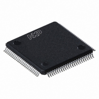
LPC1767FBD100,551 NXP Semiconductors, LPC1767FBD100,551 Datasheet - Page 273

LPC1767FBD100,551
Manufacturer Part Number
LPC1767FBD100,551
Description
IC ARM CORTEX MCU 512K 100-LQFP
Manufacturer
NXP Semiconductors
Series
LPC17xxr
Datasheets
1.LPC1767FBD100551.pdf
(2 pages)
2.LPC1767FBD100551.pdf
(840 pages)
3.LPC1767FBD100551.pdf
(65 pages)
Specifications of LPC1767FBD100,551
Core Processor
ARM® Cortex-M3™
Core Size
32-Bit
Speed
100MHz
Connectivity
Ethernet, I²C, IrDA, Microwire, SPI, SSI, UART/USART
Peripherals
Brown-out Detect/Reset, DMA, I²S, Motor Control PWM, POR, PWM, WDT
Number Of I /o
70
Program Memory Size
512KB (512K x 8)
Program Memory Type
FLASH
Ram Size
64K x 8
Voltage - Supply (vcc/vdd)
2.4 V ~ 3.6 V
Data Converters
A/D 8x12b, D/A 1x10b
Oscillator Type
Internal
Operating Temperature
-40°C ~ 85°C
Package / Case
100-LQFP
Processor Series
LPC17
Core
ARM Cortex M3
3rd Party Development Tools
MDK-ARM, RL-ARM, ULINK2, MCB1760, MCB1760U, MCB1760UME
For Use With
622-1005 - USB IN-CIRCUIT PROG ARM7 LPC2K
Lead Free Status / RoHS Status
Lead free / RoHS Compliant
Eeprom Size
-
Lead Free Status / Rohs Status
Details
Other names
568-4967
935289808551
935289808551
Available stocks
Company
Part Number
Manufacturer
Quantity
Price
Company:
Part Number:
LPC1767FBD100,551
Manufacturer:
NXP Semiconductors
Quantity:
10 000
- Current page: 273 of 840
- Download datasheet (6Mb)
13.1 How to read this chapter
13.2 Basic configuration
13.3 Introduction
13.4 Features
UM10360
User manual
The USB OTG controller is available in the LPC1768, LPC1766, LPC1765, LPC1758,
LPC1756, and LPC1754. On these devices, the USB controller can be configured for
device, Host, or OTG operation.
The USB controller is configured using the following registers:
This chapter describes the OTG and I
controller which integrates the (OHCI) host controller, device controller, and I
interface that is part of the USB block is intended to control an external OTG transceiver,
and is not the same as the I
USB OTG (On-The-Go) is a supplement to the USB 2.0 specification that augments the
capability of existing mobile devices and USB peripherals by adding host functionality for
connection to USB peripherals. The specification and more information on USB OTG can
be found on the USB Implementers Forum web site.
1. Power: In the PCONP register
2. Clock: The USB clock can generated using the dedicated USB PLL (PLL1) or with the
3. Pins: Select USB pins and their modes in PINSEL0 to PINSEL5 and PINMODE0 to
4. Wake-up: Activity on the USB bus port can wake up the microcontroller from
5. Interrupts: Interrupts are enabled in the NVIC using the appropriate Interrupt Set
6. Initialization: see
•
•
•
•
UM10360
Chapter 13: LPC17xx USB OTG
Rev. 2 — 19 August 2010
Remark: On reset, the USB block is disabled (PCUSB = 0).
Main PLL (PLL0). See
PINMODE5
Power-down mode (see
Enable register.
Fully compliant with On-The-Go supplement to the USB 2.0 Specification, Revision
1.0a.
Hardware support for Host Negotiation Protocol (HNP).
Includes a programmable timer required for HNP and SRP.
Supports any OTG transceiver compliant with the OTG Transceiver Specification
(CEA-2011), Rev. 1.0.
All information provided in this document is subject to legal disclaimers.
(Section
Section
Rev. 2 — 19 August 2010
8.5).
Section
2
Section 13.10.2
C peripherals described in
13.11.
(Table
4.6.1.
2
C portions of the USB 2.0 OTG dual role device
46), set bit PCUSB.
and
Section
Section
4.8.8).
19.1.
© NXP B.V. 2010. All rights reserved.
User manual
2
C. The I
273 of 840
2
C
Related parts for LPC1767FBD100,551
Image
Part Number
Description
Manufacturer
Datasheet
Request
R

Part Number:
Description:
32-bit ARM Cortex-M3 microcontroller; up to 512 kB flash and 64 kB SRAM with Ethernet, USB 2.0 Host/Device/OTG, CAN
Manufacturer:
NXP [NXP Semiconductors]
Datasheet:
Part Number:
Description:
NXP Semiconductors designed the LPC2420/2460 microcontroller around a 16-bit/32-bitARM7TDMI-S CPU core with real-time debug interfaces that include both JTAG andembedded trace
Manufacturer:
NXP Semiconductors
Datasheet:

Part Number:
Description:
NXP Semiconductors designed the LPC2458 microcontroller around a 16-bit/32-bitARM7TDMI-S CPU core with real-time debug interfaces that include both JTAG andembedded trace
Manufacturer:
NXP Semiconductors
Datasheet:
Part Number:
Description:
NXP Semiconductors designed the LPC2468 microcontroller around a 16-bit/32-bitARM7TDMI-S CPU core with real-time debug interfaces that include both JTAG andembedded trace
Manufacturer:
NXP Semiconductors
Datasheet:
Part Number:
Description:
NXP Semiconductors designed the LPC2470 microcontroller, powered by theARM7TDMI-S core, to be a highly integrated microcontroller for a wide range ofapplications that require advanced communications and high quality graphic displays
Manufacturer:
NXP Semiconductors
Datasheet:
Part Number:
Description:
NXP Semiconductors designed the LPC2478 microcontroller, powered by theARM7TDMI-S core, to be a highly integrated microcontroller for a wide range ofapplications that require advanced communications and high quality graphic displays
Manufacturer:
NXP Semiconductors
Datasheet:
Part Number:
Description:
The Philips Semiconductors XA (eXtended Architecture) family of 16-bit single-chip microcontrollers is powerful enough to easily handle the requirements of high performance embedded applications, yet inexpensive enough to compete in the market for hi
Manufacturer:
NXP Semiconductors
Datasheet:
Part Number:
Description:
The XA-S3 device is a member of Philips Semiconductors? XA(eXtended Architecture) family of high performance 16-bitsingle-chip microcontrollers
Manufacturer:
NXP Semiconductors
Datasheet:

Part Number:
Description:
The NXP BlueStreak LH75401/LH75411 family consists of two low-cost 16/32-bit System-on-Chip (SoC) devices
Manufacturer:
NXP Semiconductors
Datasheet:

Part Number:
Description:
The NXP LPC3130/3131 combine an 180 MHz ARM926EJ-S CPU core, high-speed USB2
Manufacturer:
NXP Semiconductors
Datasheet:

Part Number:
Description:
The NXP LPC3141 combine a 270 MHz ARM926EJ-S CPU core, High-speed USB 2
Manufacturer:
NXP Semiconductors

Part Number:
Description:
The NXP LPC3143 combine a 270 MHz ARM926EJ-S CPU core, High-speed USB 2
Manufacturer:
NXP Semiconductors

Part Number:
Description:
The NXP LPC3152 combines an 180 MHz ARM926EJ-S CPU core, High-speed USB 2
Manufacturer:
NXP Semiconductors

Part Number:
Description:
The NXP LPC3154 combines an 180 MHz ARM926EJ-S CPU core, High-speed USB 2
Manufacturer:
NXP Semiconductors


