EZ80F91AZ050EG Zilog, EZ80F91AZ050EG Datasheet - Page 118
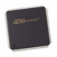
EZ80F91AZ050EG
Manufacturer Part Number
EZ80F91AZ050EG
Description
IC ACCLAIM MCU 256KB 144LQFP
Manufacturer
Zilog
Series
eZ80® Acclaim!®r
Specifications of EZ80F91AZ050EG
Core Processor
Z8
Core Size
8-Bit
Speed
50MHz
Connectivity
Ethernet, I²C, IrDA, SPI, UART/USART
Peripherals
Brown-out Detect/Reset, POR, PWM, WDT
Number Of I /o
32
Program Memory Size
256KB (256K x 8)
Program Memory Type
FLASH
Ram Size
16K x 8
Voltage - Supply (vcc/vdd)
3 V ~ 3.6 V
Oscillator Type
Internal
Operating Temperature
-40°C ~ 105°C
Package / Case
144-LQFP
Processor Series
EZ80F91x
Core
eZ80
Data Bus Width
8 bit
Data Ram Size
16 KB
Interface Type
I2C, IrDA, SPI, UART
Maximum Clock Frequency
50 MHz
Number Of Programmable I/os
32
Number Of Timers
4
Operating Supply Voltage
3 V to 3.6 V
Maximum Operating Temperature
+ 105 C
Mounting Style
SMD/SMT
Development Tools By Supplier
eZ80F910300ZCOG
Minimum Operating Temperature
- 40 C
For Use With
269-4712 - KIT DEV ENCORE 32 SERIES269-4671 - BOARD ZDOTS SBC Z80ACCLAIM PLUS269-4561 - KIT DEV FOR EZ80F91 W/C-COMPILER269-4560 - KIT DEV FOR EZ80F91 W/C-COMPILER
Lead Free Status / RoHS Status
Lead free / RoHS Compliant
Eeprom Size
-
Data Converters
-
Lead Free Status / Rohs Status
Details
Other names
269-3867
EZ80F91AZ050EG
EZ80F91AZ050EG
Available stocks
Company
Part Number
Manufacturer
Quantity
Price


PS019215-0910
Table 42. Flash Interrupt Control Register
Flash Page Select Register
The msb of this register is used to select whether I/O Flash access and PAGE ERASE
operations are directed to the 512-byte information page or to the main Flash memory
array, and also whether the information page is included in MASS ERASE operations. The
lower 7 bits are used to select one of the main 128 pages for PAGE ERASE or I/O
operations.
To perform a PAGE ERASE, the software must set the proper page value prior to setting
the page erase bit in the Flash Control Register. In addition, each access to the
Bit
Reset
CPU Access
Note: R/W = Read/Write, R = Read Only. Read resets bits [5] and [3:0].
Bit Position
[7]
DONE_IEN
[6]
ERR_IEN
[5]
DONE
[4]
[3]
WR_VIO
[2]
RP_TMO
[1]
PG_VIO
[0]
MASS_VIO
Note: The lower 32 KB block (00000h to 07FFFh) is called the Boot Block and is protected using
the external WP pin. Attempts to page erase BLK0 or mass erase Flash when WP is asserted
result in failure and signal an erase violation.
Value Description
0
1
0
1
0
1
0
0
1
0
1
0
1
0
1
R/W
Flash Erase/Row Program Done Interrupt is disabled.
Flash Erase/Row Program Done Interrupt is enabled.
Error Condition Interrupt is disabled.
Error Condition Interrupt is enabled.
Erase/Row Program Done Flag is not set.
Erase/Row Program Done Flag is set.
Reserved.
The Write Violation Error Flag is not set.
The Write Violation Error Flag is set.
The Row Program Time-Out Error Flag is not set.
The Row Program Time-Out Error Flag is set.
The Page Erase Violation Error Flag is not set.
The Page Erase Violation Error Flag is set.
The Mass Erase Violation Error Flag is not set.
The Mass Erase Violation Error Flag is set.
7
0
R/W
6
0
R
5
0
(FLASH_IRQ = 00FBh)
R
4
0
R
3
0
Product Specification
R
2
0
eZ80F91 MCU
R
1
0
Flash Memory
R
0
0
109
Related parts for EZ80F91AZ050EG
Image
Part Number
Description
Manufacturer
Datasheet
Request
R

Part Number:
Description:
Communication Controllers, ZILOG INTELLIGENT PERIPHERAL CONTROLLER (ZIP)
Manufacturer:
Zilog, Inc.
Datasheet:

Part Number:
Description:
KIT DEV FOR Z8 ENCORE 16K TO 64K
Manufacturer:
Zilog
Datasheet:

Part Number:
Description:
KIT DEV Z8 ENCORE XP 28-PIN
Manufacturer:
Zilog
Datasheet:

Part Number:
Description:
DEV KIT FOR Z8 ENCORE 8K/4K
Manufacturer:
Zilog
Datasheet:

Part Number:
Description:
KIT DEV Z8 ENCORE XP 28-PIN
Manufacturer:
Zilog
Datasheet:

Part Number:
Description:
DEV KIT FOR Z8 ENCORE 4K TO 8K
Manufacturer:
Zilog
Datasheet:
Part Number:
Description:
CMOS Z8 microcontroller. ROM 16 Kbytes, RAM 256 bytes, speed 16 MHz, 32 lines I/O, 3.0V to 5.5V
Manufacturer:
Zilog, Inc.
Datasheet:
Part Number:
Description:
Low-cost microcontroller. 512 bytes ROM, 61 bytes RAM, 8 MHz
Manufacturer:
Zilog, Inc.
Datasheet:
Part Number:
Description:
Z8 4K OTP Microcontroller
Manufacturer:
Zilog, Inc.
Datasheet:
Part Number:
Description:
CMOS SUPER8 ROMLESS MCU
Manufacturer:
Zilog, Inc.
Datasheet:
Part Number:
Description:
SL1866 CMOSZ8 OTP Microcontroller
Manufacturer:
Zilog, Inc.
Datasheet:
Part Number:
Description:
SL1866 CMOSZ8 OTP Microcontroller
Manufacturer:
Zilog, Inc.
Datasheet:
Part Number:
Description:
OTP (KB) = 1, RAM = 125, Speed = 12, I/O = 14, 8-bit Timers = 2, Comm Interfaces Other Features = Por, LV Protect, Voltage = 4.5-5.5V
Manufacturer:
Zilog, Inc.
Datasheet:
Part Number:
Description:
Manufacturer:
Zilog, Inc.
Datasheet: