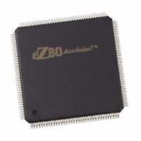
EZ80F91AZ050EG Zilog, EZ80F91AZ050EG Datasheet - Page 28

EZ80F91AZ050EG
Manufacturer Part Number
EZ80F91AZ050EG
Description
IC ACCLAIM MCU 256KB 144LQFP
Manufacturer
Zilog
Series
eZ80® Acclaim!®r
Specifications of EZ80F91AZ050EG
Core Processor
Z8
Core Size
8-Bit
Speed
50MHz
Connectivity
Ethernet, I²C, IrDA, SPI, UART/USART
Peripherals
Brown-out Detect/Reset, POR, PWM, WDT
Number Of I /o
32
Program Memory Size
256KB (256K x 8)
Program Memory Type
FLASH
Ram Size
16K x 8
Voltage - Supply (vcc/vdd)
3 V ~ 3.6 V
Oscillator Type
Internal
Operating Temperature
-40°C ~ 105°C
Package / Case
144-LQFP
Processor Series
EZ80F91x
Core
eZ80
Data Bus Width
8 bit
Data Ram Size
16 KB
Interface Type
I2C, IrDA, SPI, UART
Maximum Clock Frequency
50 MHz
Number Of Programmable I/os
32
Number Of Timers
4
Operating Supply Voltage
3 V to 3.6 V
Maximum Operating Temperature
+ 105 C
Mounting Style
SMD/SMT
Development Tools By Supplier
eZ80F910300ZCOG
Minimum Operating Temperature
- 40 C
For Use With
269-4712 - KIT DEV ENCORE 32 SERIES269-4671 - BOARD ZDOTS SBC Z80ACCLAIM PLUS269-4561 - KIT DEV FOR EZ80F91 W/C-COMPILER269-4560 - KIT DEV FOR EZ80F91 W/C-COMPILER
Lead Free Status / RoHS Status
Lead free / RoHS Compliant
Eeprom Size
-
Data Converters
-
Lead Free Status / Rohs Status
Details
Other names
269-3867
EZ80F91AZ050EG
EZ80F91AZ050EG
Available stocks
Company
Part Number
Manufacturer
Quantity
Price
- Current page: 28 of 384
- Download datasheet (3Mb)
PS019215-0910
Table 2. Pin Identification on the eZ80F91 Device (Continued)
LQFP
Pin No
106
107
108
109
110
111
112
113
BGA
Pin No Symbol
C12
C11
B12
A12
A11
B11
C10
D9
PB6
MISO
PB7
MOSI
V
SDA
SCL
PHI
V
V
SS
DD
SS
Function
GPIO Port B
SPI Master-In/
Slave-Out
GPIO Port B
SPI Master Out
Slave In
Ground
I
I
Clock
System Clock
Power Supply
Ground
2
2
C Serial Data Bidirectional
C Serial
Signal Direction Description
Bidirectional with
Schmitt-trigger
input
Bidirectional with
Schmitt-trigger
input
Bidirectional with
Schmitt-trigger
input
Bidirectional with
Schmitt-trigger
input
Bidirectional
Output
This pin is be used for GPIO. It is
individually programmed as input or
output and is also used individually as
an interrupt input. Each Port B pin,
when programmed as output is
selected to be an open-drain or open-
source output.
The MISO line is configured as an
input when the eZ80F91 device is an
SPI master device and as an output
when eZ80F91 is an SPI slave device.
This signal is multiplexed with PB6.
This pin is used for GPIO. It is
individually programmed as input or
output and is also used individually as
an interrupt input. Each Port B pin,
when programmed as output is
selected to be an open-drain or open-
source output.
The MOSI line is configured as an
output when the eZ80F91 device is an
SPI master device and as an input
when the eZ80F91 device is an SPI
slave device. This signal is
multiplexed with PB7.
Ground.
This pin carries the I
This pin is used to receive and
transmit the I
This pin is an output driven by the
internal system clock. It is used by the
system for synchronization with the
eZ80F91 device.
Power Supply.
Ground.
2
Product Specification
C clock.
Architectural Overview
2
C data signal.
19
Related parts for EZ80F91AZ050EG
Image
Part Number
Description
Manufacturer
Datasheet
Request
R

Part Number:
Description:
Communication Controllers, ZILOG INTELLIGENT PERIPHERAL CONTROLLER (ZIP)
Manufacturer:
Zilog, Inc.
Datasheet:

Part Number:
Description:
KIT DEV FOR Z8 ENCORE 16K TO 64K
Manufacturer:
Zilog
Datasheet:

Part Number:
Description:
KIT DEV Z8 ENCORE XP 28-PIN
Manufacturer:
Zilog
Datasheet:

Part Number:
Description:
DEV KIT FOR Z8 ENCORE 8K/4K
Manufacturer:
Zilog
Datasheet:

Part Number:
Description:
KIT DEV Z8 ENCORE XP 28-PIN
Manufacturer:
Zilog
Datasheet:

Part Number:
Description:
DEV KIT FOR Z8 ENCORE 4K TO 8K
Manufacturer:
Zilog
Datasheet:

Part Number:
Description:
CMOS Z8 microcontroller. ROM 16 Kbytes, RAM 256 bytes, speed 16 MHz, 32 lines I/O, 3.0V to 5.5V
Manufacturer:
Zilog, Inc.
Datasheet:

Part Number:
Description:
Low-cost microcontroller. 512 bytes ROM, 61 bytes RAM, 8 MHz
Manufacturer:
Zilog, Inc.
Datasheet:

Part Number:
Description:
Z8 4K OTP Microcontroller
Manufacturer:
Zilog, Inc.
Datasheet:

Part Number:
Description:
CMOS SUPER8 ROMLESS MCU
Manufacturer:
Zilog, Inc.
Datasheet:

Part Number:
Description:
SL1866 CMOSZ8 OTP Microcontroller
Manufacturer:
Zilog, Inc.
Datasheet:

Part Number:
Description:
SL1866 CMOSZ8 OTP Microcontroller
Manufacturer:
Zilog, Inc.
Datasheet:

Part Number:
Description:
OTP (KB) = 1, RAM = 125, Speed = 12, I/O = 14, 8-bit Timers = 2, Comm Interfaces Other Features = Por, LV Protect, Voltage = 4.5-5.5V
Manufacturer:
Zilog, Inc.
Datasheet:

Part Number:
Description:
Manufacturer:
Zilog, Inc.
Datasheet:


