EZ80F91AZ050EG Zilog, EZ80F91AZ050EG Datasheet - Page 60
EZ80F91AZ050EG
Manufacturer Part Number
EZ80F91AZ050EG
Description
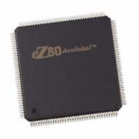
IC ACCLAIM MCU 256KB 144LQFP
Manufacturer
Zilog
Series
eZ80® Acclaim!®r
Specifications of EZ80F91AZ050EG
Core Processor
Z8
Core Size
8-Bit
Speed
50MHz
Connectivity
Ethernet, I²C, IrDA, SPI, UART/USART
Peripherals
Brown-out Detect/Reset, POR, PWM, WDT
Number Of I /o
32
Program Memory Size
256KB (256K x 8)
Program Memory Type
FLASH
Ram Size
16K x 8
Voltage - Supply (vcc/vdd)
3 V ~ 3.6 V
Oscillator Type
Internal
Operating Temperature
-40°C ~ 105°C
Package / Case
144-LQFP
Processor Series
EZ80F91x
Core
eZ80
Data Bus Width
8 bit
Data Ram Size
16 KB
Interface Type
I2C, IrDA, SPI, UART
Maximum Clock Frequency
50 MHz
Number Of Programmable I/os
32
Number Of Timers
4
Operating Supply Voltage
3 V to 3.6 V
Maximum Operating Temperature
+ 105 C
Mounting Style
SMD/SMT
Development Tools By Supplier
eZ80F910300ZCOG
Minimum Operating Temperature
- 40 C
For Use With
269-4712 - KIT DEV ENCORE 32 SERIES269-4671 - BOARD ZDOTS SBC Z80ACCLAIM PLUS269-4561 - KIT DEV FOR EZ80F91 W/C-COMPILER269-4560 - KIT DEV FOR EZ80F91 W/C-COMPILER
Lead Free Status / RoHS Status
Lead free / RoHS Compliant
Eeprom Size
-
Data Converters
-
Lead Free Status / Rohs Status
Details
Other names
269-3867
EZ80F91AZ050EG
EZ80F91AZ050EG
Available stocks
Company
Part Number
Manufacturer
Quantity
Price


PS019215-0910
an external pull-up resistor must connect the pin to the supply voltage. Writing 0 to the
Port x Data register outputs a Low at the pin. Writing 1 to the Port x Data register results in
high-impedance output.
GPIO Mode 4—Open Source
The port pin is configured as open-source I/O. The GPIO pins do not feature an internal
pull-down to the supply ground. To employ the GPIO pin in OPEN-SOURCE mode, an
external pull-down resistor must connect the pin to the supply ground. Writing 1 to the
Port x Data register outputs a High at the pin. Writing 0 to the Port x Data register results
in a high-impedance output.
GPIO Mode 5
This mode produces a high-impedance output.
GPIO Mode 6
The port pin is configured for dual edge-triggered interrupt mode. Both a rising and a
falling edge on this pin cause an interrupt request to be sent to the CPU. To select this
mode from the default mode (mode 2), you must:
1. Set Px_DR=1
2. Set Px_ALT2=1
3. Set Px_ALT1=0
4. Set Px_DDR=0
Writing a 1 to the Port x ALT0 register bit position corresponding to the interrupt request
clears the interrupt.
GPIO Mode 7—Alternate Functions
The port pin is configured to pass control over to the alternate (secondary) functions
assigned to the pin. For example, the alternate mode function for PC5 is the DSR1 input
signal to UART1 and the alternate mode function for PB4 is the timer 3 input capture.
When GPIO mode 7 is enabled, the pin output data and pin high-impedance control is
obtained from the alternate function's data output and high-impedance control,
respectively. The value in the Port x Data register produces no effect on operation. Input
signals are sampled by the system clock before being passed to the alternate input
function.
If the alternate function of a pin is an input and alternate function mode for that pin is not
enabled, the input is driven to a default non-asserted value. For example, in alternate mode
function, PC5 drives the DSR1 signal to UART1. As this signal is Low level true, the
DSR1 signal to UART1 is driven to 1 when PC5 is not in alternate mode function.
—
—
Reserved
Dual Edge Triggered
General-Purpose Input/Output
Product Specification
eZ80F91 MCU
51
Related parts for EZ80F91AZ050EG
Image
Part Number
Description
Manufacturer
Datasheet
Request
R

Part Number:
Description:
Communication Controllers, ZILOG INTELLIGENT PERIPHERAL CONTROLLER (ZIP)
Manufacturer:
Zilog, Inc.
Datasheet:

Part Number:
Description:
KIT DEV FOR Z8 ENCORE 16K TO 64K
Manufacturer:
Zilog
Datasheet:

Part Number:
Description:
KIT DEV Z8 ENCORE XP 28-PIN
Manufacturer:
Zilog
Datasheet:

Part Number:
Description:
DEV KIT FOR Z8 ENCORE 8K/4K
Manufacturer:
Zilog
Datasheet:

Part Number:
Description:
KIT DEV Z8 ENCORE XP 28-PIN
Manufacturer:
Zilog
Datasheet:

Part Number:
Description:
DEV KIT FOR Z8 ENCORE 4K TO 8K
Manufacturer:
Zilog
Datasheet:
Part Number:
Description:
CMOS Z8 microcontroller. ROM 16 Kbytes, RAM 256 bytes, speed 16 MHz, 32 lines I/O, 3.0V to 5.5V
Manufacturer:
Zilog, Inc.
Datasheet:
Part Number:
Description:
Low-cost microcontroller. 512 bytes ROM, 61 bytes RAM, 8 MHz
Manufacturer:
Zilog, Inc.
Datasheet:
Part Number:
Description:
Z8 4K OTP Microcontroller
Manufacturer:
Zilog, Inc.
Datasheet:
Part Number:
Description:
CMOS SUPER8 ROMLESS MCU
Manufacturer:
Zilog, Inc.
Datasheet:
Part Number:
Description:
SL1866 CMOSZ8 OTP Microcontroller
Manufacturer:
Zilog, Inc.
Datasheet:
Part Number:
Description:
SL1866 CMOSZ8 OTP Microcontroller
Manufacturer:
Zilog, Inc.
Datasheet:
Part Number:
Description:
OTP (KB) = 1, RAM = 125, Speed = 12, I/O = 14, 8-bit Timers = 2, Comm Interfaces Other Features = Por, LV Protect, Voltage = 4.5-5.5V
Manufacturer:
Zilog, Inc.
Datasheet:
Part Number:
Description:
Manufacturer:
Zilog, Inc.
Datasheet: