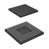
DF2552BR26DV Renesas Electronics America, DF2552BR26DV Datasheet - Page 549

DF2552BR26DV
Manufacturer Part Number
DF2552BR26DV
Description
IC H8S/2552 MCU FLASH 176-LFBGA
Manufacturer
Renesas Electronics America
Series
H8® H8S/2500r
Specifications of DF2552BR26DV
Core Processor
H8S/2000
Core Size
16-Bit
Speed
26MHz
Connectivity
I²C, SCI
Peripherals
POR, PWM, WDT
Number Of I /o
104
Program Memory Size
512KB (512K x 8)
Program Memory Type
FLASH
Ram Size
32K x 8
Voltage - Supply (vcc/vdd)
3 V ~ 5.5 V
Data Converters
A/D 16x10b; D/A 2x8b
Oscillator Type
Internal
Operating Temperature
-40°C ~ 85°C
Package / Case
176-LFBGA
Lead Free Status / RoHS Status
Lead free / RoHS Compliant
Eeprom Size
-
Available stocks
Company
Part Number
Manufacturer
Quantity
Price
Company:
Part Number:
DF2552BR26DV
Manufacturer:
Renesas Electronics America
Quantity:
10 000
- Current page: 549 of 980
- Download datasheet (6Mb)
14.4.6
This module can be operated with the clocked synchronous serial format, by setting the FS bit in
SAR to 1. When the MST bit in ICCR1 is 1, the transfer clock output from SCL is selected. When
MST is 0, the external clock input is selected.
Data Transfer Format: Figure 14.13 shows the clocked synchronous serial transfer format.
The transfer data is output from the rise to the fall of the SCL clock, and the data at the rising edge
of the SCL clock is guaranteed. The MLS bit in ICMR sets the order of data transfer, in either the
MSB first or LSB first. The output level of SDA can be changed during the transfer wait, by the
SDAO bit in ICCR2.
Transmit Operation: In transmit mode, transmit data is output from SDA, in synchronization
with the fall of the transfer clock. The transfer clock is output when MST in ICCR1 is 1, and is
(Master output)
(Master output)
(Slave output)
(Slave output)
processing
ICDRR
ICDRS
RDRF
SCL
SDA
SDA
SCL
User
Clocked Synchronous Serial Format
Figure 14.13 Clocked Synchronous Serial Transfer Format
Figure 14.12 Slave Receive Mode Operation Timing (2)
SCL
SDA
A
9
Bit 7
1
Bit 0
Bit 6
Data 1
2
Bit 1 Bit 2 Bit 3 Bit 4
Bit 5
3
Bit 4
4
Bit 3
5
[3] Set ACKBT
Bit 2
6
Bit 5 Bit 6
Rev. 6.00 Sep. 24, 2009 Page 501 of 928
Bit 1
Section 14 I
7
[3] Read ICDRR [4] Read ICDRR
Bit 0
Bit 7
8
A
2
C Bus Interface 2 (IIC2)
REJ09B0099-0600
9
Data 1
Data 2
Related parts for DF2552BR26DV
Image
Part Number
Description
Manufacturer
Datasheet
Request
R

Part Number:
Description:
KIT STARTER FOR M16C/29
Manufacturer:
Renesas Electronics America
Datasheet:

Part Number:
Description:
KIT STARTER FOR R8C/2D
Manufacturer:
Renesas Electronics America
Datasheet:

Part Number:
Description:
R0K33062P STARTER KIT
Manufacturer:
Renesas Electronics America
Datasheet:

Part Number:
Description:
KIT STARTER FOR R8C/23 E8A
Manufacturer:
Renesas Electronics America
Datasheet:

Part Number:
Description:
KIT STARTER FOR R8C/25
Manufacturer:
Renesas Electronics America
Datasheet:

Part Number:
Description:
KIT STARTER H8S2456 SHARPE DSPLY
Manufacturer:
Renesas Electronics America
Datasheet:

Part Number:
Description:
KIT STARTER FOR R8C38C
Manufacturer:
Renesas Electronics America
Datasheet:

Part Number:
Description:
KIT STARTER FOR R8C35C
Manufacturer:
Renesas Electronics America
Datasheet:

Part Number:
Description:
KIT STARTER FOR R8CL3AC+LCD APPS
Manufacturer:
Renesas Electronics America
Datasheet:

Part Number:
Description:
KIT STARTER FOR RX610
Manufacturer:
Renesas Electronics America
Datasheet:

Part Number:
Description:
KIT STARTER FOR R32C/118
Manufacturer:
Renesas Electronics America
Datasheet:

Part Number:
Description:
KIT DEV RSK-R8C/26-29
Manufacturer:
Renesas Electronics America
Datasheet:

Part Number:
Description:
KIT STARTER FOR SH7124
Manufacturer:
Renesas Electronics America
Datasheet:

Part Number:
Description:
KIT STARTER FOR H8SX/1622
Manufacturer:
Renesas Electronics America
Datasheet:

Part Number:
Description:
KIT DEV FOR SH7203
Manufacturer:
Renesas Electronics America
Datasheet:


