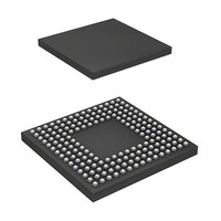
DF2552BR26DV Renesas Electronics America, DF2552BR26DV Datasheet - Page 847

DF2552BR26DV
Manufacturer Part Number
DF2552BR26DV
Description
IC H8S/2552 MCU FLASH 176-LFBGA
Manufacturer
Renesas Electronics America
Series
H8® H8S/2500r
Specifications of DF2552BR26DV
Core Processor
H8S/2000
Core Size
16-Bit
Speed
26MHz
Connectivity
I²C, SCI
Peripherals
POR, PWM, WDT
Number Of I /o
104
Program Memory Size
512KB (512K x 8)
Program Memory Type
FLASH
Ram Size
32K x 8
Voltage - Supply (vcc/vdd)
3 V ~ 5.5 V
Data Converters
A/D 16x10b; D/A 2x8b
Oscillator Type
Internal
Operating Temperature
-40°C ~ 85°C
Package / Case
176-LFBGA
Lead Free Status / RoHS Status
Lead free / RoHS Compliant
Eeprom Size
-
Available stocks
Company
Part Number
Manufacturer
Quantity
Price
Company:
Part Number:
DF2552BR26DV
Manufacturer:
Renesas Electronics America
Quantity:
10 000
- Current page: 847 of 980
- Download datasheet (6Mb)
Section 22 Power-Down Modes
22.2
Medium-Speed Mode
In high-speed mode, when the SCK2 to SCK0 bits in SCKCR are set to 1, the operating mode
changes to medium-speed mode as soon as the current bus cycle ends. In medium-speed mode, the
CPU operates on the operating clock (φ/2, φ/4, φ/8, φ/16, or φ/32) specified by the SCK2 to SCK0
bits. The bus masters other than the CPU (DTC) also operate in medium-speed mode.
On-chip peripheral modules other than the bus masters always operate on the high-speed clock (φ).
In medium-speed mode, a bus access is executed in the specified number of states with respect to
the bus master operating clock. For example, if φ/4 is selected as the operating clock, on-chip
memory is accessed in 4 states, and internal I/O registers in 8 states.
Medium-speed mode is cleared by clearing all of bits SCK2 to SCK0 to 0. A transition is made to
high-speed mode and medium-speed mode is cleared at the end of the current bus cycle.
If a SLEEP instruction is executed when the SSBY bit in SBYCR and the LSON bit in LPWRCR
are cleared to 0, a transition is made to sleep mode. When sleep mode is cleared by an interrupt,
medium-speed mode is restored.
When the SLEEP instruction is executed with the SSBY bit = 1, LSON bit = 0, and PSS bit in
TCSR_1 (WDT_1) = 0, operation shifts to the software standby mode. When software standby
mode is cleared by an external interrupt, medium-speed mode is restored.
When the RES pin is set low and medium-speed mode is cancelled, operation shifts to the reset
state. The same applies in the case of a reset caused by overflow of the watchdog timer.
When the STBY pin is driven low, a transition is made to hardware standby mode.
Figure 22.2 shows the timing for transition to and clearance of medium-speed mode.
Rev. 6.00 Sep. 24, 2009 Page 799 of 928
REJ09B0099-0600
Related parts for DF2552BR26DV
Image
Part Number
Description
Manufacturer
Datasheet
Request
R

Part Number:
Description:
KIT STARTER FOR M16C/29
Manufacturer:
Renesas Electronics America
Datasheet:

Part Number:
Description:
KIT STARTER FOR R8C/2D
Manufacturer:
Renesas Electronics America
Datasheet:

Part Number:
Description:
R0K33062P STARTER KIT
Manufacturer:
Renesas Electronics America
Datasheet:

Part Number:
Description:
KIT STARTER FOR R8C/23 E8A
Manufacturer:
Renesas Electronics America
Datasheet:

Part Number:
Description:
KIT STARTER FOR R8C/25
Manufacturer:
Renesas Electronics America
Datasheet:

Part Number:
Description:
KIT STARTER H8S2456 SHARPE DSPLY
Manufacturer:
Renesas Electronics America
Datasheet:

Part Number:
Description:
KIT STARTER FOR R8C38C
Manufacturer:
Renesas Electronics America
Datasheet:

Part Number:
Description:
KIT STARTER FOR R8C35C
Manufacturer:
Renesas Electronics America
Datasheet:

Part Number:
Description:
KIT STARTER FOR R8CL3AC+LCD APPS
Manufacturer:
Renesas Electronics America
Datasheet:

Part Number:
Description:
KIT STARTER FOR RX610
Manufacturer:
Renesas Electronics America
Datasheet:

Part Number:
Description:
KIT STARTER FOR R32C/118
Manufacturer:
Renesas Electronics America
Datasheet:

Part Number:
Description:
KIT DEV RSK-R8C/26-29
Manufacturer:
Renesas Electronics America
Datasheet:

Part Number:
Description:
KIT STARTER FOR SH7124
Manufacturer:
Renesas Electronics America
Datasheet:

Part Number:
Description:
KIT STARTER FOR H8SX/1622
Manufacturer:
Renesas Electronics America
Datasheet:

Part Number:
Description:
KIT DEV FOR SH7203
Manufacturer:
Renesas Electronics America
Datasheet:


