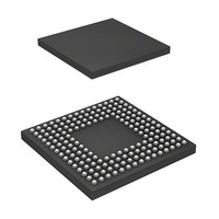
DF2552BR26DV Renesas Electronics America, DF2552BR26DV Datasheet - Page 571

DF2552BR26DV
Manufacturer Part Number
DF2552BR26DV
Description
IC H8S/2552 MCU FLASH 176-LFBGA
Manufacturer
Renesas Electronics America
Series
H8® H8S/2500r
Specifications of DF2552BR26DV
Core Processor
H8S/2000
Core Size
16-Bit
Speed
26MHz
Connectivity
I²C, SCI
Peripherals
POR, PWM, WDT
Number Of I /o
104
Program Memory Size
512KB (512K x 8)
Program Memory Type
FLASH
Ram Size
32K x 8
Voltage - Supply (vcc/vdd)
3 V ~ 5.5 V
Data Converters
A/D 16x10b; D/A 2x8b
Oscillator Type
Internal
Operating Temperature
-40°C ~ 85°C
Package / Case
176-LFBGA
Lead Free Status / RoHS Status
Lead free / RoHS Compliant
Eeprom Size
-
Available stocks
Company
Part Number
Manufacturer
Quantity
Price
Company:
Part Number:
DF2552BR26DV
Manufacturer:
Renesas Electronics America
Quantity:
10 000
- Current page: 571 of 980
- Download datasheet (6Mb)
15.5.2
In scan mode, A/D conversion is to be performed sequentially on the specified channels (four
channels maximum). The operations are as follows.
1. When the ADST bit is set to 1 by software, timer conversion start trigger, or external trigger
2. When A/D conversion for each channel is completed, the result is sequentially transferred to
3. When conversion of all the selected channels is completed, the ADF flag is set to 1. If the
4. Steps 2 to 3 are repeated as long as the ADST bit remains set to 1. When the ADST bit is
State of channel 0 (AN0)
State of channel 1 (AN1)
State of channel 2 (AN2)
State of channel 3 (AN3)
input, A/D conversion starts on the first channel in the group (AN0 when CH3 = 0 and CH2 =
0, AN4 when CH3 = 0 and CH2 = 1, AN8 when CH3 = 1 and CH2 = 0, or AN12 when CH3 =
1 and CH2 = 1).
the A/D data register corresponding to each channel.
ADIE bit is set to 1 at this time, an ADI interrupt is requested after A/D conversion ends.
Conversion of the first channel in the group starts again.
cleared to 0, A/D conversion stops and the A/D converter enters the wait state. After that,
when the ADST bit is set to 1, conversion of the first channel in the group starts again.
Figure 15.3 A/D Conversion Timing (Single-Chip Mode, Channel 1 Selected)
ADIE
ADST
ADF
ADDRA
ADDRB
ADDRC
ADDRD
Scan Mode
Note: * Vertical arrows ( ) indicate instructions executed by software.
A/D
conversion
starts
Idle
Idle
Idle
Idle
A/D conversion
Set *
Set*
1
Idle
Clear*
Read conversion result *
A/D conversion result 1
Rev. 6.00 Sep. 24, 2009 Page 523 of 928
A/D conversion
Set*
2
Section 15 A/D Converter
Read conversion result *
A/D conversion result 2
Clear*
Idle
REJ09B0099-0600
Related parts for DF2552BR26DV
Image
Part Number
Description
Manufacturer
Datasheet
Request
R

Part Number:
Description:
KIT STARTER FOR M16C/29
Manufacturer:
Renesas Electronics America
Datasheet:

Part Number:
Description:
KIT STARTER FOR R8C/2D
Manufacturer:
Renesas Electronics America
Datasheet:

Part Number:
Description:
R0K33062P STARTER KIT
Manufacturer:
Renesas Electronics America
Datasheet:

Part Number:
Description:
KIT STARTER FOR R8C/23 E8A
Manufacturer:
Renesas Electronics America
Datasheet:

Part Number:
Description:
KIT STARTER FOR R8C/25
Manufacturer:
Renesas Electronics America
Datasheet:

Part Number:
Description:
KIT STARTER H8S2456 SHARPE DSPLY
Manufacturer:
Renesas Electronics America
Datasheet:

Part Number:
Description:
KIT STARTER FOR R8C38C
Manufacturer:
Renesas Electronics America
Datasheet:

Part Number:
Description:
KIT STARTER FOR R8C35C
Manufacturer:
Renesas Electronics America
Datasheet:

Part Number:
Description:
KIT STARTER FOR R8CL3AC+LCD APPS
Manufacturer:
Renesas Electronics America
Datasheet:

Part Number:
Description:
KIT STARTER FOR RX610
Manufacturer:
Renesas Electronics America
Datasheet:

Part Number:
Description:
KIT STARTER FOR R32C/118
Manufacturer:
Renesas Electronics America
Datasheet:

Part Number:
Description:
KIT DEV RSK-R8C/26-29
Manufacturer:
Renesas Electronics America
Datasheet:

Part Number:
Description:
KIT STARTER FOR SH7124
Manufacturer:
Renesas Electronics America
Datasheet:

Part Number:
Description:
KIT STARTER FOR H8SX/1622
Manufacturer:
Renesas Electronics America
Datasheet:

Part Number:
Description:
KIT DEV FOR SH7203
Manufacturer:
Renesas Electronics America
Datasheet:


