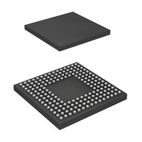
DF2552BR26DV Renesas Electronics America, DF2552BR26DV Datasheet - Page 745

DF2552BR26DV
Manufacturer Part Number
DF2552BR26DV
Description
IC H8S/2552 MCU FLASH 176-LFBGA
Manufacturer
Renesas Electronics America
Series
H8® H8S/2500r
Specifications of DF2552BR26DV
Core Processor
H8S/2000
Core Size
16-Bit
Speed
26MHz
Connectivity
I²C, SCI
Peripherals
POR, PWM, WDT
Number Of I /o
104
Program Memory Size
512KB (512K x 8)
Program Memory Type
FLASH
Ram Size
32K x 8
Voltage - Supply (vcc/vdd)
3 V ~ 5.5 V
Data Converters
A/D 16x10b; D/A 2x8b
Oscillator Type
Internal
Operating Temperature
-40°C ~ 85°C
Package / Case
176-LFBGA
Lead Free Status / RoHS Status
Lead free / RoHS Compliant
Eeprom Size
-
Available stocks
Company
Part Number
Manufacturer
Quantity
Price
Company:
Part Number:
DF2552BR26DV
Manufacturer:
Renesas Electronics America
Quantity:
10 000
- Current page: 745 of 980
- Download datasheet (6Mb)
Table 20.6 Division of User MAT Area
Legend:
*: Don’t care
20.3.4
FVACR modifies the space from which the vector table data of the NMI interrupts is read.
Normally the vector table data is read from the address spaces from H'00001C to H'00001F.
However, the vector table can be read from the internal I/O register (FVADRR to FVADRL) by
the FVACR setting. FVACR is initialized to H'00 at a power-on reset or in hardware standby
mode.
All interrupts including NMI must be prohibited in the programming/erasing processing or during
downloading on-chip program. When the NMI interrupt is necessary such as in the system error
processing, FVACR and FVADRR to FVADRL must be set and the interrupt exception
processing routine must be set in the on-chip RAM space or in the external space.
RAM Area
H'FFD000 to H'FFDFFF RAM area (4 kbytes) 0
H'000000 to H'000FFF
H'001000 to H'001FFF
H'002000 to H'002FFF
H'003000 to H'003FFF
H'004000 to H'004FFF
H'005000 to H'005FFF
H'006000 to H'006FFF
H'007000 to H'007FFF
Bit
7
Bit Name
FVCHGE
Flash Vector Address Control Register (FVACR)
Initial
Value
0
Block Name
EB0 (4 kbytes)
EB1 (4 kbytes)
EB2 (4 kbytes)
EB3 (4 kbytes)
EB4 (4 kbytes)
EB5 (4 kbytes)
EB6 (4 kbytes)
EB7 (4 kbytes)
R/W
R/W
Description
Vector Switch Function Valid
Selects whether the function for modifying the space from
which the vector table data is read is valid or invalid. When
FVCHGE = 1, the vector table data can be read from the
internal I/O register (FVADRR to FVADRL).
0: Function for modifying the space from which the vector
1: Function for modifying the space from which the vector
table data is read is invalid (Initial value)
table data is read is valid
RAMS
1
1
1
1
1
1
1
1
RAM2
*
0
0
0
0
1
1
1
1
Rev. 6.00 Sep. 24, 2009 Page 697 of 928
RAM1
*
0
0
1
1
0
0
1
1
Section 20 Flash Memory
REJ09B0099-0600
RAM0
*
0
1
0
1
0
1
0
1
Related parts for DF2552BR26DV
Image
Part Number
Description
Manufacturer
Datasheet
Request
R

Part Number:
Description:
KIT STARTER FOR M16C/29
Manufacturer:
Renesas Electronics America
Datasheet:

Part Number:
Description:
KIT STARTER FOR R8C/2D
Manufacturer:
Renesas Electronics America
Datasheet:

Part Number:
Description:
R0K33062P STARTER KIT
Manufacturer:
Renesas Electronics America
Datasheet:

Part Number:
Description:
KIT STARTER FOR R8C/23 E8A
Manufacturer:
Renesas Electronics America
Datasheet:

Part Number:
Description:
KIT STARTER FOR R8C/25
Manufacturer:
Renesas Electronics America
Datasheet:

Part Number:
Description:
KIT STARTER H8S2456 SHARPE DSPLY
Manufacturer:
Renesas Electronics America
Datasheet:

Part Number:
Description:
KIT STARTER FOR R8C38C
Manufacturer:
Renesas Electronics America
Datasheet:

Part Number:
Description:
KIT STARTER FOR R8C35C
Manufacturer:
Renesas Electronics America
Datasheet:

Part Number:
Description:
KIT STARTER FOR R8CL3AC+LCD APPS
Manufacturer:
Renesas Electronics America
Datasheet:

Part Number:
Description:
KIT STARTER FOR RX610
Manufacturer:
Renesas Electronics America
Datasheet:

Part Number:
Description:
KIT STARTER FOR R32C/118
Manufacturer:
Renesas Electronics America
Datasheet:

Part Number:
Description:
KIT DEV RSK-R8C/26-29
Manufacturer:
Renesas Electronics America
Datasheet:

Part Number:
Description:
KIT STARTER FOR SH7124
Manufacturer:
Renesas Electronics America
Datasheet:

Part Number:
Description:
KIT STARTER FOR H8SX/1622
Manufacturer:
Renesas Electronics America
Datasheet:

Part Number:
Description:
KIT DEV FOR SH7203
Manufacturer:
Renesas Electronics America
Datasheet:


