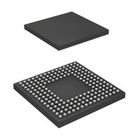
DF2552BR26DV Renesas Electronics America, DF2552BR26DV Datasheet - Page 601

DF2552BR26DV
Manufacturer Part Number
DF2552BR26DV
Description
IC H8S/2552 MCU FLASH 176-LFBGA
Manufacturer
Renesas Electronics America
Series
H8® H8S/2500r
Specifications of DF2552BR26DV
Core Processor
H8S/2000
Core Size
16-Bit
Speed
26MHz
Connectivity
I²C, SCI
Peripherals
POR, PWM, WDT
Number Of I /o
104
Program Memory Size
512KB (512K x 8)
Program Memory Type
FLASH
Ram Size
32K x 8
Voltage - Supply (vcc/vdd)
3 V ~ 5.5 V
Data Converters
A/D 16x10b; D/A 2x8b
Oscillator Type
Internal
Operating Temperature
-40°C ~ 85°C
Package / Case
176-LFBGA
Lead Free Status / RoHS Status
Lead free / RoHS Compliant
Eeprom Size
-
Available stocks
Company
Part Number
Manufacturer
Quantity
Price
Company:
Part Number:
DF2552BR26DV
Manufacturer:
Renesas Electronics America
Quantity:
10 000
- Current page: 601 of 980
- Download datasheet (6Mb)
(2)
In the case of data read (H'3, H'7), data in the data buffer of the slave unit is read in the master
unit. In the case of data write (H'B or H'F) or command write (H'A or H'E), data received in the
slave unit is processed in accordance with the operation specification of the slave unit.
Notes: 1. The user can select data and commands freely in accordance with the system.
(3)
In the case of the locked address read (H'4 or H'5), the address (12 bits) of the master unit which
issues lock instruction is configured in bytes shown in figure 17.4.
Data Command Transfer (Control Bits: Read (H'3, H'7), Write (H'A, H'B, H'E, H'F))
Locked Address Read (Control Bits: H′4, H′5)
Notes: 1. Since this LSI can support up to mode 2, bits 6 and 7 are fixed to 10.
2. H'3, H'A, or H'B may lock depending on the communications condition and status.
2. The value of bit 4 can be selected by the STE bit in the IEBus master unit address register 1 (IEAR1).
3. The slave receive buffer is a buffer which is accessed during data write
4. The slave transmit buffer is a buffer which is accessed during data read
MSB
(control bits: H'8, H'A, H'B, H'E, H'F).
In this LSI, the slave receive buffer corresponds to the IEBus receive buffer register (IERBR);
and bit 2 is the value of the RxRDY flag in the IEBus receive status register (IERSR).
(control bits: H'3, H'7).
In this LSI, the slave transmit buffer corresponds to the IEBus transmit buffer register (IETBR)
when SRQ = 1 in the IEBus general flag register (IEFLG); and bit 1 is a value which reverses the
TxRDY flag in the IEBus transmit/runaway status register (IETSR).
Bit 7
Figure 17.3 Bit Configuration of Slave Status (SSR)
Bit
Bit 7,
bit 6
Bit 5
Bit 4*
Bit 3
Bit 2
Bit 1*
Bit 0*
Bit 6
2
3
4
Value Description
Bit 5
00
01
10
11
0
0
1
0
0
1
0
1
0
1
Mode 0
Mode 1
Mode 2
For future use
Fixed 0
Slave transmission halted
Slave transmission enabled
Fixed 0
Unit is unlocked
Unit is locked
Slave receive buffer is empty
Slave receive buffer is not empty
Slave transmit buffer is empty
Slave transmit buffer is not empty
Bit 4
Bit 3
Section 17 IEBus™ Controller (IEB) [H8S/2552 Group]
Indicates the highest mode
supported by a unit. *
Bit 2
Rev. 6.00 Sep. 24, 2009 Page 553 of 928
Bit 1
1
Bit 0
LSB
REJ09B0099-0600
Related parts for DF2552BR26DV
Image
Part Number
Description
Manufacturer
Datasheet
Request
R

Part Number:
Description:
KIT STARTER FOR M16C/29
Manufacturer:
Renesas Electronics America
Datasheet:

Part Number:
Description:
KIT STARTER FOR R8C/2D
Manufacturer:
Renesas Electronics America
Datasheet:

Part Number:
Description:
R0K33062P STARTER KIT
Manufacturer:
Renesas Electronics America
Datasheet:

Part Number:
Description:
KIT STARTER FOR R8C/23 E8A
Manufacturer:
Renesas Electronics America
Datasheet:

Part Number:
Description:
KIT STARTER FOR R8C/25
Manufacturer:
Renesas Electronics America
Datasheet:

Part Number:
Description:
KIT STARTER H8S2456 SHARPE DSPLY
Manufacturer:
Renesas Electronics America
Datasheet:

Part Number:
Description:
KIT STARTER FOR R8C38C
Manufacturer:
Renesas Electronics America
Datasheet:

Part Number:
Description:
KIT STARTER FOR R8C35C
Manufacturer:
Renesas Electronics America
Datasheet:

Part Number:
Description:
KIT STARTER FOR R8CL3AC+LCD APPS
Manufacturer:
Renesas Electronics America
Datasheet:

Part Number:
Description:
KIT STARTER FOR RX610
Manufacturer:
Renesas Electronics America
Datasheet:

Part Number:
Description:
KIT STARTER FOR R32C/118
Manufacturer:
Renesas Electronics America
Datasheet:

Part Number:
Description:
KIT DEV RSK-R8C/26-29
Manufacturer:
Renesas Electronics America
Datasheet:

Part Number:
Description:
KIT STARTER FOR SH7124
Manufacturer:
Renesas Electronics America
Datasheet:

Part Number:
Description:
KIT STARTER FOR H8SX/1622
Manufacturer:
Renesas Electronics America
Datasheet:

Part Number:
Description:
KIT DEV FOR SH7203
Manufacturer:
Renesas Electronics America
Datasheet:


