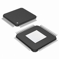
PIC24FJ256DA210T-I/BG Microchip Technology, PIC24FJ256DA210T-I/BG Datasheet - Page 141

PIC24FJ256DA210T-I/BG
Manufacturer Part Number
PIC24FJ256DA210T-I/BG
Description
16-bit, 256KB Flash, 96K RAM, USB, Graphics 121 XBGA 10x10x1.20mm T/R
Manufacturer
Microchip Technology
Series
PIC® 24Fr
Specifications of PIC24FJ256DA210T-I/BG
Core Processor
PIC
Core Size
16-Bit
Speed
32MHz
Connectivity
I²C, IrDA, SPI, UART/USART, USB OTG
Peripherals
Brown-out Detect/Reset, GFX, LVD, POR, PWM, WDT
Number Of I /o
84
Program Memory Size
256KB (85.5K x 24)
Program Memory Type
FLASH
Ram Size
96K x 8
Voltage - Supply (vcc/vdd)
2.2 V ~ 3.6 V
Data Converters
A/D 24x10b
Oscillator Type
Internal
Operating Temperature
-40°C ~ 85°C
Package / Case
121-TFBGA
Lead Free Status / RoHS Status
Lead free / RoHS Compliant
Eeprom Size
-
Lead Free Status / RoHS Status
Lead free / RoHS Compliant
Available stocks
Company
Part Number
Manufacturer
Quantity
Price
Company:
Part Number:
PIC24FJ256DA210T-I/BG
Manufacturer:
Microchip Technology
Quantity:
10 000
- Current page: 141 of 408
- Download datasheet (4Mb)
8.0
The oscillator system for PIC24FJ256DA210 family
devices has the following features:
• A total of four external and internal oscillator options
FIGURE 8-1:
2010 Microchip Technology Inc.
Note:
as clock sources, providing 11 different clock modes
Note 1:
SOSCO
SOSCI
OSCO
OSCI
OSCILLATOR
CONFIGURATION
This data sheet summarizes the features
of this group of PIC24F devices. It is not
intended to be a comprehensive reference
source. For more information, refer to the
“PIC24F
Section 6. “Oscillator” (DS39700). The
information in this data sheet supersedes
the information in the FRM.
Refer to Figure 8-2 for more information on the 96 MHz PLL block.
Primary Oscillator
Oscillator
Oscillator
Secondary Oscillator
Family
PIC24FJ256DA210 FAMILY CLOCK DIAGRAM
LPRC
FRC
(nominal)
SOSCEN
Enable
Oscillator
8 MHz
Reference
31 kHz (nominal)
96 MHz PLL
PLLDIV<2:0>
Manual”,
PIC24FJ256DA210 FAMILY
CLKDIV<10:8>
(1)
PLL and
DIV
1/16
GCLKDIV<6:0>
CPDIV<1:0>
PIC24FJ256DA210 Family
8 MHz/
4 MHz
• An on-chip PLL block to boost internal operating
• Software controllable switching between various
• Software controllable postscaler for selective
• A Fail-Safe Clock Monitor (FSCM) that detects
• A separate and independently configurable system
A simplified diagram of the oscillator system is shown
in Figure 8-1.
ECPLL,FRCPLL
XTPLL, HSPLL
frequency on select internal and external oscillator
sources, and to provide a precise clock source for
peripherals, such as USB and graphics
clock sources
clocking of CPU for system power savings
clock failure and permits safe application recovery
or shutdown
clock output for synchronizing external hardware
XT, HS, EC
48/96 MHz Clock for Graphics Controller Module
FRCDIV
LPFRC
SOSC
LPRC
Clock Control Logic
FRC
Fail-Safe
Monitor
Clock
CLKDIV<14:12>
Clock for Display Interface
Reference Clock
Clock Source Option
Generator
48 MHz USB Clock
REFOCON<15:8>
for Other Modules
DS39969B-page 141
Peripherals
WDT
REFO
CLKO
CPU
Related parts for PIC24FJ256DA210T-I/BG
Image
Part Number
Description
Manufacturer
Datasheet
Request
R

Part Number:
Description:
Manufacturer:
Microchip Technology Inc.
Datasheet:

Part Number:
Description:
Manufacturer:
Microchip Technology Inc.
Datasheet:

Part Number:
Description:
Manufacturer:
Microchip Technology Inc.
Datasheet:

Part Number:
Description:
Manufacturer:
Microchip Technology Inc.
Datasheet:

Part Number:
Description:
Manufacturer:
Microchip Technology Inc.
Datasheet:

Part Number:
Description:
Manufacturer:
Microchip Technology Inc.
Datasheet:

Part Number:
Description:
Manufacturer:
Microchip Technology Inc.
Datasheet:

Part Number:
Description:
Manufacturer:
Microchip Technology Inc.
Datasheet:


