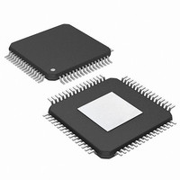
PIC24FJ256DA210T-I/BG Microchip Technology, PIC24FJ256DA210T-I/BG Datasheet - Page 204

PIC24FJ256DA210T-I/BG
Manufacturer Part Number
PIC24FJ256DA210T-I/BG
Description
16-bit, 256KB Flash, 96K RAM, USB, Graphics 121 XBGA 10x10x1.20mm T/R
Manufacturer
Microchip Technology
Series
PIC® 24Fr
Specifications of PIC24FJ256DA210T-I/BG
Core Processor
PIC
Core Size
16-Bit
Speed
32MHz
Connectivity
I²C, IrDA, SPI, UART/USART, USB OTG
Peripherals
Brown-out Detect/Reset, GFX, LVD, POR, PWM, WDT
Number Of I /o
84
Program Memory Size
256KB (85.5K x 24)
Program Memory Type
FLASH
Ram Size
96K x 8
Voltage - Supply (vcc/vdd)
2.2 V ~ 3.6 V
Data Converters
A/D 24x10b
Oscillator Type
Internal
Operating Temperature
-40°C ~ 85°C
Package / Case
121-TFBGA
Lead Free Status / RoHS Status
Lead free / RoHS Compliant
Eeprom Size
-
Lead Free Status / RoHS Status
Lead free / RoHS Compliant
Available stocks
Company
Part Number
Manufacturer
Quantity
Price
Company:
Part Number:
PIC24FJ256DA210T-I/BG
Manufacturer:
Microchip Technology
Quantity:
10 000
- Current page: 204 of 408
- Download datasheet (4Mb)
PIC24FJ256DA210 FAMILY
FIGURE 14-2:
14.3.1
The PWM period is specified by writing to PRy, the
Timer Period register. The PWM period can be
calculated using Equation 14-1.
EQUATION 14-1:
DS39969B-page 204
Note:
Trigger and
Sync Sources
OC Clock
Sources
Note 1: The OCx outputs must be assigned to an available RPn pin before use. See Section 10.4 “Peripheral Pin
Note 1:
2: The OCFA/OCFB fault inputs must be assigned to an available RPn/RPIn pin before use. See Section 10.4
PWM PERIOD
A PRy value of N will produce a PWM period of N + 1 time base count cycles. For example, a value of 7
written into the PRy register will yield a period consisting of 8 time base cycles.
TRIGMODE
Select (PPS)” for more information.
“Peripheral Pin Select (PPS)” for more information.
SYNCSELx
TRIGSTAT
OCTSELx
OCTRIG
Based on T
Trigger and
OUTPUT COMPARE BLOCK DIAGRAM (DOUBLE-BUFFERED, 16-BIT PWM MODE)
Sync Logic
CALCULATING THE PWM PERIOD
Select
Clock
PWM Period = [(PRy) + 1 • T
where:
PWM Frequency = 1/[PWM Period]
Reset
CY
= T
Match Event
OSC
Increment
Reset
* 2; Doze mode and PLL are disabled.
DCB<1:0> Buffers
OCxRS Buffer
Comparator
Comparator
OCxR and
DCB<1:0>
OCxCON1
OCxCON2
OCxR and
OCxTMR
OCxRS
CY
Rollover/Reset
Rollover/Reset
• (Timer Prescale Value)
(1)
Match
Event
Match
Event
Rollover
OC Output and
Fault Logic
OCx Interrupt
OCMx
OCINV
OCTRIS
FLTOUT
FLTTRIEN
FLTMD
ENFLT<2:0>
OCFLT<2:0>
DCB<1:0>
2010 Microchip Technology Inc.
OCFA/OCFB
OCx Pin
(1)
(2)
Related parts for PIC24FJ256DA210T-I/BG
Image
Part Number
Description
Manufacturer
Datasheet
Request
R

Part Number:
Description:
Manufacturer:
Microchip Technology Inc.
Datasheet:

Part Number:
Description:
Manufacturer:
Microchip Technology Inc.
Datasheet:

Part Number:
Description:
Manufacturer:
Microchip Technology Inc.
Datasheet:

Part Number:
Description:
Manufacturer:
Microchip Technology Inc.
Datasheet:

Part Number:
Description:
Manufacturer:
Microchip Technology Inc.
Datasheet:

Part Number:
Description:
Manufacturer:
Microchip Technology Inc.
Datasheet:

Part Number:
Description:
Manufacturer:
Microchip Technology Inc.
Datasheet:

Part Number:
Description:
Manufacturer:
Microchip Technology Inc.
Datasheet:


