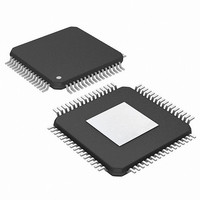
PIC24FJ256DA210T-I/BG Microchip Technology, PIC24FJ256DA210T-I/BG Datasheet - Page 17

PIC24FJ256DA210T-I/BG
Manufacturer Part Number
PIC24FJ256DA210T-I/BG
Description
16-bit, 256KB Flash, 96K RAM, USB, Graphics 121 XBGA 10x10x1.20mm T/R
Manufacturer
Microchip Technology
Series
PIC® 24Fr
Specifications of PIC24FJ256DA210T-I/BG
Core Processor
PIC
Core Size
16-Bit
Speed
32MHz
Connectivity
I²C, IrDA, SPI, UART/USART, USB OTG
Peripherals
Brown-out Detect/Reset, GFX, LVD, POR, PWM, WDT
Number Of I /o
84
Program Memory Size
256KB (85.5K x 24)
Program Memory Type
FLASH
Ram Size
96K x 8
Voltage - Supply (vcc/vdd)
2.2 V ~ 3.6 V
Data Converters
A/D 24x10b
Oscillator Type
Internal
Operating Temperature
-40°C ~ 85°C
Package / Case
121-TFBGA
Lead Free Status / RoHS Status
Lead free / RoHS Compliant
Eeprom Size
-
Lead Free Status / RoHS Status
Lead free / RoHS Compliant
Available stocks
Company
Part Number
Manufacturer
Quantity
Price
Company:
Part Number:
PIC24FJ256DA210T-I/BG
Manufacturer:
Microchip Technology
Quantity:
10 000
- Current page: 17 of 408
- Download datasheet (4Mb)
1.5
Devices in the PIC24FJ256DA210 family are available
in 64-pin and 100-pin packages. The general block
diagram for all devices is shown in Figure 1-1.
The devices are differentiated from each other in seven
ways:
1.
2.
3.
4.
2010 Microchip Technology Inc.
Flash program memory (128 Kbytes for
PIC24FJ128DAXXX devices and 256 Kbytes
for PIC24FJ256DAXXX devices).
Data memory (24 Kbytes for PIC24FJXXXDA1XX
devices, and 96 Kbytes for PIC24FJXXXDA2XX
devices).
Available I/O pins and ports (52 pins on 6 ports
for PIC24FJXXXDAX06 devices and 84 pins on
7 ports for PIC24FJXXXDAX10 devices).
Available Interrupt-on-Change Notification (ICN)
inputs (52 on PIC24FJXXXDAx06 devices and
84 on PIC24FJXXXDAX10 devices).
Details on Individual Family
Members
PIC24FJ256DA210 FAMILY
5.
6.
7.
All other features for devices in this family are identical.
These are summarized in Table 1-1 and Table 1-2.
A
PIC24FJ256DA210 family devices, sorted by function,
is shown in Table 1-1. Note that this table shows the pin
location of individual peripheral features and not how
they are multiplexed on the same pin. This information
is provided in the pinout diagrams in the beginning of
the data sheet. Multiplexed features are sorted by the
priority given to a feature, with the highest priority
peripheral being listed first.
list
Available
PIC24FJXXXDAX06 devices and 44 pins on
PIC24FJXXXDAX10 devices).
Analog channels for ADC (16 channels for
PIC24FJXXXDAX06 devices and 24 channels
for PIC24FJxxxDAx10 devices).
EPMP module (available in PIC24FJXXXDAX10
devices and not in PIC24FJXXXDAX06 devices).
of
the
remappable
pin
features
pins
available
DS39969B-page 17
(29
pins
on
on
the
Related parts for PIC24FJ256DA210T-I/BG
Image
Part Number
Description
Manufacturer
Datasheet
Request
R

Part Number:
Description:
Manufacturer:
Microchip Technology Inc.
Datasheet:

Part Number:
Description:
Manufacturer:
Microchip Technology Inc.
Datasheet:

Part Number:
Description:
Manufacturer:
Microchip Technology Inc.
Datasheet:

Part Number:
Description:
Manufacturer:
Microchip Technology Inc.
Datasheet:

Part Number:
Description:
Manufacturer:
Microchip Technology Inc.
Datasheet:

Part Number:
Description:
Manufacturer:
Microchip Technology Inc.
Datasheet:

Part Number:
Description:
Manufacturer:
Microchip Technology Inc.
Datasheet:

Part Number:
Description:
Manufacturer:
Microchip Technology Inc.
Datasheet:


