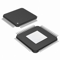
PIC24FJ256DA210T-I/BG Microchip Technology, PIC24FJ256DA210T-I/BG Datasheet - Page 352

PIC24FJ256DA210T-I/BG
Manufacturer Part Number
PIC24FJ256DA210T-I/BG
Description
16-bit, 256KB Flash, 96K RAM, USB, Graphics 121 XBGA 10x10x1.20mm T/R
Manufacturer
Microchip Technology
Series
PIC® 24Fr
Specifications of PIC24FJ256DA210T-I/BG
Core Processor
PIC
Core Size
16-Bit
Speed
32MHz
Connectivity
I²C, IrDA, SPI, UART/USART, USB OTG
Peripherals
Brown-out Detect/Reset, GFX, LVD, POR, PWM, WDT
Number Of I /o
84
Program Memory Size
256KB (85.5K x 24)
Program Memory Type
FLASH
Ram Size
96K x 8
Voltage - Supply (vcc/vdd)
2.2 V ~ 3.6 V
Data Converters
A/D 24x10b
Oscillator Type
Internal
Operating Temperature
-40°C ~ 85°C
Package / Case
121-TFBGA
Lead Free Status / RoHS Status
Lead free / RoHS Compliant
Eeprom Size
-
Lead Free Status / RoHS Status
Lead free / RoHS Compliant
Available stocks
Company
Part Number
Manufacturer
Quantity
Price
Company:
Part Number:
PIC24FJ256DA210T-I/BG
Manufacturer:
Microchip Technology
Quantity:
10 000
- Current page: 352 of 408
- Download datasheet (4Mb)
PIC24FJ256DA210 FAMILY
REGISTER 27-3:
REGISTER 27-4:
DS39969B-page 352
bit 11-10
bit 9-8
bit 7-0
Note 1:
bit 23
bit 15
bit 7
Legend:
R = Readable bit
-n = Value at POR
bit 23-16
bit 15-0
reserved
reserved
U-0
r-1
r-1
—
2:
3:
Unimplemented in 64-pin devices, maintain at ‘1’.
Ensure that the SCLKI pin is made a digital input while using this configuration, see Table 10-1.
Regardless of WPCFG status, if WPEND = 1 or if WPFP corresponds to the Configuration Word’s page,
the Configuration Word’s page is protected.
WUTSEL<1:0>: Voltage Regulator Standby Mode Wake-up Time Select bits
11 = Default regulator start-up time is used
01 = Fast regulator start-up time is used
x0 = Reserved; do not use
SOSCSEL<1:0>: SOSC Selection Configuration bits
11 = Secondary oscillator is in Default (high drive strength) Oscillator mode
10 = Reserved; do not use
01 = Secondary oscillator is in Low-Power (low drive strength) Oscillator mode
00 = External clock (SCLKI) or Digital I/O mode
WPFP<7:0>: Write Protected Code Segment Boundary Page bits
Designates the 512 instruction words page boundary of the protected code segment.
If WPEND = 1:
Specifies the lower page boundary of the code-protected segment; the last page being the last
implemented page in the device.
If WPEND = 0:
Specifies the upper page boundary of the code-protected segment; Page 0 being the lower boundary.
Unimplemented: Read as ‘0’
Reserved: Always maintain as ‘1’
reserved
reserved
U-0
r-1
r-1
—
CW3: FLASH CONFIGURATION WORD 3 (CONTINUED)
CW4: FLASH CONFIGURATION WORD 4
r = Reserved bit
W = Writable bit
‘1’ = Bit is set
reserved
reserved
U-0
r-1
r-1
—
reserved
reserved
U-0
r-1
r-1
—
U = Unimplemented bit, read as ‘0’
‘0’ = Bit is cleared
reserved
reserved
(2)
U-0
r-1
r-1
—
reserved
reserved
U-0
r-1
r-1
—
2010 Microchip Technology Inc.
x = Bit is unknown
reserved
reserved
U-0
r-1
r-1
—
reserved
reserved
U-0
r-1
r-1
—
bit 16
bit 8
bit 0
Related parts for PIC24FJ256DA210T-I/BG
Image
Part Number
Description
Manufacturer
Datasheet
Request
R

Part Number:
Description:
Manufacturer:
Microchip Technology Inc.
Datasheet:

Part Number:
Description:
Manufacturer:
Microchip Technology Inc.
Datasheet:

Part Number:
Description:
Manufacturer:
Microchip Technology Inc.
Datasheet:

Part Number:
Description:
Manufacturer:
Microchip Technology Inc.
Datasheet:

Part Number:
Description:
Manufacturer:
Microchip Technology Inc.
Datasheet:

Part Number:
Description:
Manufacturer:
Microchip Technology Inc.
Datasheet:

Part Number:
Description:
Manufacturer:
Microchip Technology Inc.
Datasheet:

Part Number:
Description:
Manufacturer:
Microchip Technology Inc.
Datasheet:


