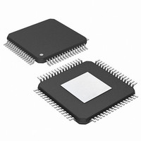
PIC24FJ256DA210T-I/BG Microchip Technology, PIC24FJ256DA210T-I/BG Datasheet - Page 157

PIC24FJ256DA210T-I/BG
Manufacturer Part Number
PIC24FJ256DA210T-I/BG
Description
16-bit, 256KB Flash, 96K RAM, USB, Graphics 121 XBGA 10x10x1.20mm T/R
Manufacturer
Microchip Technology
Series
PIC® 24Fr
Specifications of PIC24FJ256DA210T-I/BG
Core Processor
PIC
Core Size
16-Bit
Speed
32MHz
Connectivity
I²C, IrDA, SPI, UART/USART, USB OTG
Peripherals
Brown-out Detect/Reset, GFX, LVD, POR, PWM, WDT
Number Of I /o
84
Program Memory Size
256KB (85.5K x 24)
Program Memory Type
FLASH
Ram Size
96K x 8
Voltage - Supply (vcc/vdd)
2.2 V ~ 3.6 V
Data Converters
A/D 24x10b
Oscillator Type
Internal
Operating Temperature
-40°C ~ 85°C
Package / Case
121-TFBGA
Lead Free Status / RoHS Status
Lead free / RoHS Compliant
Eeprom Size
-
Lead Free Status / RoHS Status
Lead free / RoHS Compliant
Available stocks
Company
Part Number
Manufacturer
Quantity
Price
Company:
Part Number:
PIC24FJ256DA210T-I/BG
Manufacturer:
Microchip Technology
Quantity:
10 000
- Current page: 157 of 408
- Download datasheet (4Mb)
10.0
All of the device pins (except V
OSCI/CLKI) are shared between the peripherals and
the parallel I/O ports. All I/O input ports feature Schmitt
Trigger (ST) inputs for improved noise immunity.
10.1
A parallel I/O port that shares a pin with a peripheral is,
in general, subservient to the peripheral. The periph-
eral’s output buffer data and control signals are
provided to a pair of multiplexers. The multiplexers
select whether the peripheral or the associated port
has ownership of the output data and control signals of
the I/O pin. The logic also prevents “loop through”, in
which a port’s digital output can drive the input of a
peripheral that shares the same pin. Figure 10-1 shows
how ports are shared with other peripherals and the
associated I/O pin to which they are connected.
FIGURE 10-1:
2010 Microchip Technology Inc.
Note:
I/O PORTS
Parallel I/O (PIO) Ports
This data sheet summarizes the features
of this group of PIC24F devices. It is not
intended to be a comprehensive reference
source. For more information, refer to the
“PIC24F
Section 12. “I/O Ports with Peripheral
Pin Select (PPS)” (DS39711). The infor-
mation in this data sheet supersedes the
information in the FRM.
Read TRIS
Data Bus
WR TRIS
WR LAT +
WR PORT
Read LAT
Read PORT
Family
BLOCK DIAGRAM OF A TYPICAL SHARED PORT STRUCTURE
Peripheral Input Data
Peripheral Module Enable
Peripheral Output Enable
Peripheral Output Data
Peripheral Module
PIO Module
Reference
TRIS Latch
DD
Data Latch
D
D
CK
CK
, V
SS
Q
Q
, MCLR and
Manual”,
PIC24FJ256DA210 FAMILY
Output Multiplexers
When a peripheral is enabled and the peripheral is
actively driving an associated pin, the use of the pin as
a general purpose output pin is disabled. The I/O pin
may be read, but the output driver for the parallel port
bit will be disabled. If a peripheral is enabled, but the
peripheral is not actively driving a pin, that pin may be
driven by a port.
All port pins have three registers directly associated
with their operation as digital I/O and one register asso-
ciated with their operation as analog input. The Data
Direction register (TRISx) determines whether the pin
is an input or an output. If the data direction bit is a ‘1’,
then the pin is an input. All port pins are defined as
inputs after a Reset. Reads from the Output Latch reg-
ister (LATx), read the latch; writes to the latch, write the
latch. Reads from the port (PORTx), read the port pins;
writes to the port pins, write the latch.
Any bit and its associated data and control registers
that are not valid for a particular device will be
disabled. That means the corresponding LATx and
TRISx registers, and the port pin will read as zeros.
When a pin is shared with another peripheral or func-
tion that is defined as an input only, it is regarded as a
dedicated port because there is no other competing
source of inputs.
1
0
1
0
Output Enable
Output Data
Input Data
I/O
I/O Pin
DS39969B-page 157
Related parts for PIC24FJ256DA210T-I/BG
Image
Part Number
Description
Manufacturer
Datasheet
Request
R

Part Number:
Description:
Manufacturer:
Microchip Technology Inc.
Datasheet:

Part Number:
Description:
Manufacturer:
Microchip Technology Inc.
Datasheet:

Part Number:
Description:
Manufacturer:
Microchip Technology Inc.
Datasheet:

Part Number:
Description:
Manufacturer:
Microchip Technology Inc.
Datasheet:

Part Number:
Description:
Manufacturer:
Microchip Technology Inc.
Datasheet:

Part Number:
Description:
Manufacturer:
Microchip Technology Inc.
Datasheet:

Part Number:
Description:
Manufacturer:
Microchip Technology Inc.
Datasheet:

Part Number:
Description:
Manufacturer:
Microchip Technology Inc.
Datasheet:


