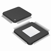
PIC24FJ256DA210T-I/BG Microchip Technology, PIC24FJ256DA210T-I/BG Datasheet - Page 320

PIC24FJ256DA210T-I/BG
Manufacturer Part Number
PIC24FJ256DA210T-I/BG
Description
16-bit, 256KB Flash, 96K RAM, USB, Graphics 121 XBGA 10x10x1.20mm T/R
Manufacturer
Microchip Technology
Series
PIC® 24Fr
Specifications of PIC24FJ256DA210T-I/BG
Core Processor
PIC
Core Size
16-Bit
Speed
32MHz
Connectivity
I²C, IrDA, SPI, UART/USART, USB OTG
Peripherals
Brown-out Detect/Reset, GFX, LVD, POR, PWM, WDT
Number Of I /o
84
Program Memory Size
256KB (85.5K x 24)
Program Memory Type
FLASH
Ram Size
96K x 8
Voltage - Supply (vcc/vdd)
2.2 V ~ 3.6 V
Data Converters
A/D 24x10b
Oscillator Type
Internal
Operating Temperature
-40°C ~ 85°C
Package / Case
121-TFBGA
Lead Free Status / RoHS Status
Lead free / RoHS Compliant
Eeprom Size
-
Lead Free Status / RoHS Status
Lead free / RoHS Compliant
Available stocks
Company
Part Number
Manufacturer
Quantity
Price
Company:
Part Number:
PIC24FJ256DA210T-I/BG
Manufacturer:
Microchip Technology
Quantity:
10 000
- Current page: 320 of 408
- Download datasheet (4Mb)
PIC24FJ256DA210 FAMILY
REGISTER 22-26: G1CLUTWR: COLOR LOOK-UP TABLE (CLUT) MEMORY WRITE DATA
REGISTER 22-27: G1CLUTRD: COLOR LOOK-UP TABLE (CLUT) MEMORY READ DATA REGISTER
DS39969B-page 320
bit 15
bit 7
Legend:
R = Readable bit
-n = Value at POR
bit 15-0
bit 15
bit 7
Legend:
R = Readable bit
-n = Value at POR
bit 15-0
CLUTWR15
CLUTRD15
CLUTWR7
CLUTRD7
R-0, HSC
R-0, HSC
R/W-0
R/W-0
CLUTRD<15:0>: Color Look-up Table Memory Read Data bits
This register contains the most recent read from the CLUT memory pointed to by the CLUTADR bits
(G1CLUT<7:0>). Reading of the CLUT memory is triggered when the CLUTTRD bit (G1CLUT<9>) goes
from ‘0’ to ‘1’. Refer to the “PIC24F Family Reference Manual”, Section 43. “Graphics Controller Module
(GFX)” for details on reading entries from the CLUT.
CLUTWR<15:0>: Color Look-up Table Memory Write Data bits
A write to this register triggers a write to the CLUT memory at the address pointed to by the CLUTADR
bits. A word write or a high byte write to this register triggers a write to the CLUT memory at the address
pointed to by CLUTADR. Low byte write to this register will only update the G1CLUTWR<7:0> and no
write to CLUT memory will be triggered. During power-up and power-down of the display, the most
recent data written to this register will be used to control the timing of the GPWR signal. Refer to the
“PIC24F Family Reference Manual”, Section 43. “Graphics Controller Module (GFX)” for details on
writing entries to the CLUT.
CLUTWR14
CLUTRD14
CLUTWR6
CLUTRD6
R-0, HSC
R-0, HSC
R/W-0
R/W-0
REGISTER
HSC = Hardware Settable/Clearable bit
W = Writable bit
‘1’ = Bit is set
W = Writable bit
‘1’ = Bit is set
CLUTRD13
CLUTWR13
CLUTRD5
CLUTWR5
R-0, HSC
R-0, HSC
R/W-0
R/W-0
CLUTRD12
CLUTRD4
R-0, HSC
R-0, HSC
CLUTWR12
CLUTWR4
R/W-0
R/W-0
U = Unimplemented bit, read as ‘0’
‘0’ = Bit is cleared
CLUTRD11
U = Unimplemented bit, read as ‘0’
‘0’ = Bit is cleared
CLUTRD3
R-0, HSC
R-0, HSC
CLUTWR11
CLUTWR3
R/W-0
R/W-0
CLUTRD10
CLUTWR10
CLUTRD2
CLUTWR2
R-0, HSC
R-0, HSC
R/W-0
R/W-0
2010 Microchip Technology Inc.
x = Bit is unknown
x = Bit is unknown
CLUTWR9
CLUTWR1
CLUTRD9
CLUTRD1
R-0, HSC
R-0, HSC
R/W-0
R/W-0
CLUTRD8
CLUTWR8
CLUTWR0
R-0, HSC
CLUTRD0
R-0, HSC
R/W-0
R/W-0
bit 8
bit 0
bit 8
bit 0
Related parts for PIC24FJ256DA210T-I/BG
Image
Part Number
Description
Manufacturer
Datasheet
Request
R

Part Number:
Description:
Manufacturer:
Microchip Technology Inc.
Datasheet:

Part Number:
Description:
Manufacturer:
Microchip Technology Inc.
Datasheet:

Part Number:
Description:
Manufacturer:
Microchip Technology Inc.
Datasheet:

Part Number:
Description:
Manufacturer:
Microchip Technology Inc.
Datasheet:

Part Number:
Description:
Manufacturer:
Microchip Technology Inc.
Datasheet:

Part Number:
Description:
Manufacturer:
Microchip Technology Inc.
Datasheet:

Part Number:
Description:
Manufacturer:
Microchip Technology Inc.
Datasheet:

Part Number:
Description:
Manufacturer:
Microchip Technology Inc.
Datasheet:


