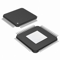
PIC24FJ256DA210T-I/BG Microchip Technology, PIC24FJ256DA210T-I/BG Datasheet - Page 350

PIC24FJ256DA210T-I/BG
Manufacturer Part Number
PIC24FJ256DA210T-I/BG
Description
16-bit, 256KB Flash, 96K RAM, USB, Graphics 121 XBGA 10x10x1.20mm T/R
Manufacturer
Microchip Technology
Series
PIC® 24Fr
Specifications of PIC24FJ256DA210T-I/BG
Core Processor
PIC
Core Size
16-Bit
Speed
32MHz
Connectivity
I²C, IrDA, SPI, UART/USART, USB OTG
Peripherals
Brown-out Detect/Reset, GFX, LVD, POR, PWM, WDT
Number Of I /o
84
Program Memory Size
256KB (85.5K x 24)
Program Memory Type
FLASH
Ram Size
96K x 8
Voltage - Supply (vcc/vdd)
2.2 V ~ 3.6 V
Data Converters
A/D 24x10b
Oscillator Type
Internal
Operating Temperature
-40°C ~ 85°C
Package / Case
121-TFBGA
Lead Free Status / RoHS Status
Lead free / RoHS Compliant
Eeprom Size
-
Lead Free Status / RoHS Status
Lead free / RoHS Compliant
Available stocks
Company
Part Number
Manufacturer
Quantity
Price
Company:
Part Number:
PIC24FJ256DA210T-I/BG
Manufacturer:
Microchip Technology
Quantity:
10 000
- Current page: 350 of 408
- Download datasheet (4Mb)
PIC24FJ256DA210 FAMILY
REGISTER 27-2:
DS39969B-page 350
bit 23
bit 15
bit 7
Legend:
R = Readable bit
-n = Value at POR
bit 23-16
bit 15
bit 14-12
bit 11
bit 10-8
bit 7-6
bit 5
FCKSM1
R/PO-1
R/PO-1
IESO
U-0
—
Unimplemented: Read as ‘1’
IESO: Internal External Switchover bit
1 = IESO mode (Two-Speed Start-up) is enabled
0 = IESO mode (Two-Speed Start-up) is disabled
PLLDIV<2:0>: 96 MHz PLL Prescaler Select bits
111 = Oscillator input is divided by 12 (48 MHz input)
110 = Oscillator input is divided by 8 (32 MHz input)
101 = Oscillator input is divided by 6 (24 MHz input)
100 = Oscillator input is divided by 5 (20 MHz input)
011 = Oscillator input is divided by 4 (16 MHz input)
010 = Oscillator input is divided by 3 (12 MHz input)
001 = Oscillator input is divided by 2 (8 MHz input)
000 = Oscillator input is used directly (4 MHz input)
PLL96MHZ: 96 MHz PLL Start-Up Enable bit
1 = 96 MHz PLL is enabled automatically on start-up
0 = 96 MHz PLL is software controlled (can be enabled by setting the PLLEN bit in CLKDIV<5>)
FNOSC<2:0>: Initial Oscillator Select bits
111 = Fast RC Oscillator with Postscaler (FRCDIV)
110 = Reserved
101 = Low-Power RC Oscillator (LPRC)
100 = Secondary Oscillator (SOSC)
011 = Primary Oscillator with PLL module (XTPLL, HSPLL, ECPLL)
010 = Primary Oscillator (XT, HS, EC)
001 = Fast RC Oscillator with Postscaler and PLL module (FRCPLL)
000 = Fast RC Oscillator (FRC)
FCKSM<1:0>: Clock Switching and Fail-Safe Clock Monitor Configuration bits
1x = Clock switching and Fail-Safe Clock Monitor are disabled
01 = Clock switching is enabled, Fail-Safe Clock Monitor is disabled
00 = Clock switching is enabled, Fail-Safe Clock Monitor is enabled
OSCIOFCN: OSCO Pin Configuration bit
If POSCMD<1:0> = 11 or 00:
1 = OSCO/CLKO/RC15 functions as CLKO (F
0 = OSCO/CLKO/RC15 functions as port I/O (RC15)
If POSCMD<1:0> = 10 or 01:
OSCIOFCN has no effect on OSCO/CLKO/RC15.
FCKSM0
PLLDIV2
R/PO-1
R/PO-1
U-0
—
CW2: FLASH CONFIGURATION WORD 2
r = Reserved bit
W = Writable bit
‘1’ = Bit is set
OSCIOFCN
PLLDIV1
R/PO-1
R/PO-1
U-0
—
IOL1WAY
PLLDIV0
R/PO-1
R/PO-1
U-0
—
U = Unimplemented bit, read as ‘0’
‘0’ = Bit is cleared
PLL96MHZ
reserved
OSC
R/PO-1
U-0
r-1
—
/2)
FNOSC2
reserved
R/PO-1
U-0
r-1
—
2010 Microchip Technology Inc.
x = Bit is unknown
POSCMD1
FNOSC1
R/PO-1
R/PO-1
U-0
—
POSCMD0
FNOSC0
R/PO-1
R/PO-1
U-0
—
bit 16
bit 8
bit 0
Related parts for PIC24FJ256DA210T-I/BG
Image
Part Number
Description
Manufacturer
Datasheet
Request
R

Part Number:
Description:
Manufacturer:
Microchip Technology Inc.
Datasheet:

Part Number:
Description:
Manufacturer:
Microchip Technology Inc.
Datasheet:

Part Number:
Description:
Manufacturer:
Microchip Technology Inc.
Datasheet:

Part Number:
Description:
Manufacturer:
Microchip Technology Inc.
Datasheet:

Part Number:
Description:
Manufacturer:
Microchip Technology Inc.
Datasheet:

Part Number:
Description:
Manufacturer:
Microchip Technology Inc.
Datasheet:

Part Number:
Description:
Manufacturer:
Microchip Technology Inc.
Datasheet:

Part Number:
Description:
Manufacturer:
Microchip Technology Inc.
Datasheet:


