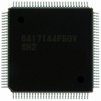
HD6417144F50V Renesas Electronics America, HD6417144F50V Datasheet - Page 108

HD6417144F50V
Manufacturer Part Number
HD6417144F50V
Description
IC SUPERH MCU ROMLESS 112QFP
Manufacturer
Renesas Electronics America
Series
SuperH® SH7144r
Datasheet
1.HD64F7144F50V.pdf
(932 pages)
Specifications of HD6417144F50V
Core Processor
SH-2
Core Size
32-Bit
Speed
50MHz
Connectivity
EBI/EMI, I²C, SCI
Peripherals
DMA, POR, PWM, WDT
Number Of I /o
74
Program Memory Type
ROMless
Ram Size
8K x 8
Voltage - Supply (vcc/vdd)
3 V ~ 3.6 V
Data Converters
A/D 8x10b
Oscillator Type
Internal
Operating Temperature
-20°C ~ 75°C
Package / Case
112-QFP
For Use With
HS0005KCU11H - EMULATOR E10A-USB H8S(X),SH2(A)EDK7145 - DEV EVALUATION KIT SH7145
Lead Free Status / RoHS Status
Lead free / RoHS Compliant
Eeprom Size
-
Program Memory Size
-
Available stocks
Company
Part Number
Manufacturer
Quantity
Price
Company:
Part Number:
HD6417144F50V
Manufacturer:
Renesas Electronics America
Quantity:
10 000
- Current page: 108 of 932
- Download datasheet (6Mb)
5. Exception Processing
5.1.2
The exception processing sources are detected and begin processing according to the timing
shown in table 5.2.
Table 5.2
When exception processing starts, the CPU operates as follows:
1. Exception processing triggered by reset:
2. Exception processing triggered by address errors, interrupts and instructions:
Rev.4.00 Mar. 27, 2008 Page 62 of 882
REJ09B0108-0400
Exception
Reset
Address error
Interrupts
Instructions
The initial values of the program counter (PC) and stack pointer (SP) are fetched from the
exception processing vector table (PC and SP are respectively the H'00000000 and
H'00000004 addresses for power-on resets and the H'00000008 and H'0000000C addresses for
manual resets). See section 5.1.3, Exception Processing Vector Table, for more information.
H'00000000 is then written to the vector base register (VBR), and H'F (B'1111) is written to
the interrupt mask bits (I3 to I0) of the status register (SR). The program begins running from
the PC address fetched from the exception processing vector table.
SR and PC are saved to the stack indicated by R15. For interrupt exception processing, the
interrupt priority level is written to the SR’s interrupt mask bits (I3 to I0). For address error
and instruction exception processing, the I3 to I0 bits are not affected. The start address is then
fetched from the exception processing vector table and the program begins running from that
address.
3. Instructions that rewrite the PC: JMP, JSR, BRA, BSR, RTS, RTE, BT, BF, TRAPA,
Exception Processing Operations
BF/S, BT/S, BSRF, and BRAF.
Timing for Exception Source Detection and Start of Exception Processing
Source
Power-on reset
Manual reset
Trap instruction
General illegal
instructions
Illegal slot
instructions
Timing of Source Detection and Start of Processing
Starts when the RES pin changes from low to high or when
WDT overflows.
Starts when the MRES pin changes from low to high.
Detected when instruction is decoded and starts when the
execution of the previous instruction is completed.
Starts from the execution of a TRAPA instruction.
Starts from the decoding of undefined code anytime except
after a delayed branch instruction (delay slot).
Starts from the decoding of undefined code placed in a delayed
branch instruction (delay slot) or of instructions that rewrite the
PC.
Related parts for HD6417144F50V
Image
Part Number
Description
Manufacturer
Datasheet
Request
R

Part Number:
Description:
KIT STARTER FOR M16C/29
Manufacturer:
Renesas Electronics America
Datasheet:

Part Number:
Description:
KIT STARTER FOR R8C/2D
Manufacturer:
Renesas Electronics America
Datasheet:

Part Number:
Description:
R0K33062P STARTER KIT
Manufacturer:
Renesas Electronics America
Datasheet:

Part Number:
Description:
KIT STARTER FOR R8C/23 E8A
Manufacturer:
Renesas Electronics America
Datasheet:

Part Number:
Description:
KIT STARTER FOR R8C/25
Manufacturer:
Renesas Electronics America
Datasheet:

Part Number:
Description:
KIT STARTER H8S2456 SHARPE DSPLY
Manufacturer:
Renesas Electronics America
Datasheet:

Part Number:
Description:
KIT STARTER FOR R8C38C
Manufacturer:
Renesas Electronics America
Datasheet:

Part Number:
Description:
KIT STARTER FOR R8C35C
Manufacturer:
Renesas Electronics America
Datasheet:

Part Number:
Description:
KIT STARTER FOR R8CL3AC+LCD APPS
Manufacturer:
Renesas Electronics America
Datasheet:

Part Number:
Description:
KIT STARTER FOR RX610
Manufacturer:
Renesas Electronics America
Datasheet:

Part Number:
Description:
KIT STARTER FOR R32C/118
Manufacturer:
Renesas Electronics America
Datasheet:

Part Number:
Description:
KIT DEV RSK-R8C/26-29
Manufacturer:
Renesas Electronics America
Datasheet:

Part Number:
Description:
KIT STARTER FOR SH7124
Manufacturer:
Renesas Electronics America
Datasheet:

Part Number:
Description:
KIT STARTER FOR H8SX/1622
Manufacturer:
Renesas Electronics America
Datasheet:

Part Number:
Description:
KIT DEV FOR SH7203
Manufacturer:
Renesas Electronics America
Datasheet:


