HD6417144F50V Renesas Electronics America, HD6417144F50V Datasheet - Page 574
HD6417144F50V
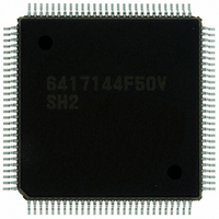
Manufacturer Part Number
HD6417144F50V
Description
IC SUPERH MCU ROMLESS 112QFP
Manufacturer
Renesas Electronics America
Series
SuperH® SH7144r
Datasheet
1.HD64F7144F50V.pdf
(932 pages)
Specifications of HD6417144F50V
Core Processor
SH-2
Core Size
32-Bit
Speed
50MHz
Connectivity
EBI/EMI, I²C, SCI
Peripherals
DMA, POR, PWM, WDT
Number Of I /o
74
Program Memory Type
ROMless
Ram Size
8K x 8
Voltage - Supply (vcc/vdd)
3 V ~ 3.6 V
Data Converters
A/D 8x10b
Oscillator Type
Internal
Operating Temperature
-20°C ~ 75°C
Package / Case
112-QFP
For Use With
HS0005KCU11H - EMULATOR E10A-USB H8S(X),SH2(A)EDK7145 - DEV EVALUATION KIT SH7145
Lead Free Status / RoHS Status
Lead free / RoHS Compliant
Eeprom Size
-
Program Memory Size
-
Available stocks
Company
Part Number
Manufacturer
Quantity
Price
Company:

Part Number:
HD6417144F50V
Manufacturer:
Renesas Electronics America
Quantity:
10 000


14. I
14.5
1. In master mode, when the instruction that generates the start condition is issued immediately
2. The following two conditions apply to the start of the next transfer: take note when reading
3. In synchronization with the internal clock, SCL and SDA are output with the timing shown in
Table 14.8 I
Note:
Rev.4.00 Mar. 27, 2008 Page 528 of 882
REJ09B0108-0400
Item
SCL-output cycle time
SCL-output high-pulse width
SCL-output low-pulse width
SDA-output bus-free time
Start-condition-output hold time
Output setup time for re-transmission of start
condition
Setup time for output of the stop condition
Setup time for the output of data (master)
Setup time for the output of data (slave)
Data-output hold time
after the instruction that generates the stop condition, neither the start condition nor the stop
condition will be correctly output. For the consecutive output of the start condition and stop
condition, read the port after issuing the instruction that generates the start condition, and make
sure that the levels on both SCL and SDA are low. Then issue the instruction that generates the
stop condition. Note that SCL may not have completely reached its low level when BBSY
becomes 1.
from/writing to ICDR.
⎯ ICE = 1, TRS = 1, and data is written to ICDR (including automatic transfer from ICDRT
⎯ ICE = 1, TRS = 0, and data is read from ICDR (including automatic transfer from ICDRS
table 14.8. The timing on the bus is determined by the rise/fall times of the signals, and these
are affected by the bus-load’s capacitance, series resistance, and parallel resistance.
2
C Bus Interface (IIC) Option
to ICDRS)
to ICDRR)
*
Usage Notes
When the IICX is 0, 6 t
2
C Bus Timing (output of SCL and SDA)
pcyc
. When IICX is 1, 12 t
Symbol
t
t
t
t
t
t
t
t
t
SCLO
SCLHO
SCLLO
BUFO
STAHO
STASO
STOSO
SDASO
SDAHO
pcyc
Output Timing
28 t
0.5 t
0.5 t
0.5 t
0.5 t
1 t
0.5 t
1 t
1 t
t
3 t
pcyc
.
SCLO
SCLLO
SCLL
pcyc
*)
pcyc
SCLO
SCLO
SCLO
SCLO
SCLO
−(6 t
to 256 t
−3 t
−1 t
−1 t
+2 t
pcyc
pcyc
pcyc
pcyc
pcyc
or 12
pcyc
Unit
ns
ns
ns
ns
ns
ns
ns
ns
ns
ns
Remarks
Related parts for HD6417144F50V
Image
Part Number
Description
Manufacturer
Datasheet
Request
R

Part Number:
Description:
KIT STARTER FOR M16C/29
Manufacturer:
Renesas Electronics America
Datasheet:

Part Number:
Description:
KIT STARTER FOR R8C/2D
Manufacturer:
Renesas Electronics America
Datasheet:

Part Number:
Description:
R0K33062P STARTER KIT
Manufacturer:
Renesas Electronics America
Datasheet:

Part Number:
Description:
KIT STARTER FOR R8C/23 E8A
Manufacturer:
Renesas Electronics America
Datasheet:

Part Number:
Description:
KIT STARTER FOR R8C/25
Manufacturer:
Renesas Electronics America
Datasheet:

Part Number:
Description:
KIT STARTER H8S2456 SHARPE DSPLY
Manufacturer:
Renesas Electronics America
Datasheet:

Part Number:
Description:
KIT STARTER FOR R8C38C
Manufacturer:
Renesas Electronics America
Datasheet:

Part Number:
Description:
KIT STARTER FOR R8C35C
Manufacturer:
Renesas Electronics America
Datasheet:

Part Number:
Description:
KIT STARTER FOR R8CL3AC+LCD APPS
Manufacturer:
Renesas Electronics America
Datasheet:
Part Number:
Description:
KIT STARTER FOR RX610
Manufacturer:
Renesas Electronics America
Datasheet:

Part Number:
Description:
KIT STARTER FOR R32C/118
Manufacturer:
Renesas Electronics America
Datasheet:

Part Number:
Description:
KIT DEV RSK-R8C/26-29
Manufacturer:
Renesas Electronics America
Datasheet:

Part Number:
Description:
KIT STARTER FOR SH7124
Manufacturer:
Renesas Electronics America
Datasheet:

Part Number:
Description:
KIT STARTER FOR H8SX/1622
Manufacturer:
Renesas Electronics America
Datasheet:

Part Number:
Description:
KIT DEV FOR SH7203
Manufacturer:
Renesas Electronics America
Datasheet: