HD6417144F50V Renesas Electronics America, HD6417144F50V Datasheet - Page 339
HD6417144F50V
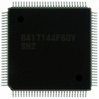
Manufacturer Part Number
HD6417144F50V
Description
IC SUPERH MCU ROMLESS 112QFP
Manufacturer
Renesas Electronics America
Series
SuperH® SH7144r
Datasheet
1.HD64F7144F50V.pdf
(932 pages)
Specifications of HD6417144F50V
Core Processor
SH-2
Core Size
32-Bit
Speed
50MHz
Connectivity
EBI/EMI, I²C, SCI
Peripherals
DMA, POR, PWM, WDT
Number Of I /o
74
Program Memory Type
ROMless
Ram Size
8K x 8
Voltage - Supply (vcc/vdd)
3 V ~ 3.6 V
Data Converters
A/D 8x10b
Oscillator Type
Internal
Operating Temperature
-20°C ~ 75°C
Package / Case
112-QFP
For Use With
HS0005KCU11H - EMULATOR E10A-USB H8S(X),SH2(A)EDK7145 - DEV EVALUATION KIT SH7145
Lead Free Status / RoHS Status
Lead free / RoHS Compliant
Eeprom Size
-
Program Memory Size
-
Available stocks
Company
Part Number
Manufacturer
Quantity
Price
Company:

Part Number:
HD6417144F50V
Manufacturer:
Renesas Electronics America
Quantity:
10 000


3. Initialization
Table 11.41 Registers and Counters Requiring Initialization
Note: The TGRC_3 set value must be the sum of 1/2 the PWM carrier cycle set in TCBR and
4. PWM Output Level Setting
5. Dead Time Setting
Register/Counter
TGRC_3
TDDR
TCBR
TGRD_3, TGRC_4, TGRD_4
TCNT_4
In complementary PWM mode, there are six registers that must be initialized.
Before setting complementary PWM mode with bits MD3 to MD0 in the timer mode register
(TMDR), the following initial register values must be set.
TGRC_3 operates as the buffer register for TGRA_3, and should be set with 1/2 the PWM
carrier cycle + dead time Td. The timer cycle buffer register (TCBR) operates as the buffer
register for the timer cycle data register (TCDR), and should be set with 1/2 the PWM carrier
cycle. Set dead time Td in the timer dead time data register (TDDR).
Set the respective initial PWM duty values in buffer registers TGRD_3, TGRC_4, and
TGRD_4.
The values set in the five buffer registers excluding TDDR are transferred simultaneously to
the corresponding compare registers when complementary PWM mode is set.
Set TCNT_4 to H'0000 before setting complementary PWM mode.
In complementary PWM mode, the PWM pulse output level is set with bits OLSN and OLSP
in the timer output control register (TOCR).
The output level can be set for each of the three positive phases and three negative phases of 6-
phase output.
Complementary PWM mode should be cleared before setting or changing output levels.
In complementary PWM mode, PWM pulses are output with a non-overlapping relationship
between the positive and negative phases. This non-overlap time is called the dead time.
The non-overlap time is set in the timer dead time data register (TDDR). The value set in
TDDR is used as the TCNT_3 counter start value, and creates non-overlap between TCNT_3
and TCNT_4. Complementary PWM mode should be cleared before changing the contents of
TDDR.
dead time Td set in TDDR.
Set Value
Dead time Td
1/2 PWM carrier cycle
Initial PWM duty value for each phase
H'0000
1/2 PWM carrier cycle + dead time Td
11.
Rev.4.00 Mar. 27, 2008 Page 293 of 882
Multi-Function Timer Pulse Unit (MTU)
REJ09B0108-0400
Related parts for HD6417144F50V
Image
Part Number
Description
Manufacturer
Datasheet
Request
R

Part Number:
Description:
KIT STARTER FOR M16C/29
Manufacturer:
Renesas Electronics America
Datasheet:

Part Number:
Description:
KIT STARTER FOR R8C/2D
Manufacturer:
Renesas Electronics America
Datasheet:

Part Number:
Description:
R0K33062P STARTER KIT
Manufacturer:
Renesas Electronics America
Datasheet:

Part Number:
Description:
KIT STARTER FOR R8C/23 E8A
Manufacturer:
Renesas Electronics America
Datasheet:

Part Number:
Description:
KIT STARTER FOR R8C/25
Manufacturer:
Renesas Electronics America
Datasheet:

Part Number:
Description:
KIT STARTER H8S2456 SHARPE DSPLY
Manufacturer:
Renesas Electronics America
Datasheet:

Part Number:
Description:
KIT STARTER FOR R8C38C
Manufacturer:
Renesas Electronics America
Datasheet:

Part Number:
Description:
KIT STARTER FOR R8C35C
Manufacturer:
Renesas Electronics America
Datasheet:

Part Number:
Description:
KIT STARTER FOR R8CL3AC+LCD APPS
Manufacturer:
Renesas Electronics America
Datasheet:
Part Number:
Description:
KIT STARTER FOR RX610
Manufacturer:
Renesas Electronics America
Datasheet:

Part Number:
Description:
KIT STARTER FOR R32C/118
Manufacturer:
Renesas Electronics America
Datasheet:

Part Number:
Description:
KIT DEV RSK-R8C/26-29
Manufacturer:
Renesas Electronics America
Datasheet:

Part Number:
Description:
KIT STARTER FOR SH7124
Manufacturer:
Renesas Electronics America
Datasheet:

Part Number:
Description:
KIT STARTER FOR H8SX/1622
Manufacturer:
Renesas Electronics America
Datasheet:

Part Number:
Description:
KIT DEV FOR SH7203
Manufacturer:
Renesas Electronics America
Datasheet: