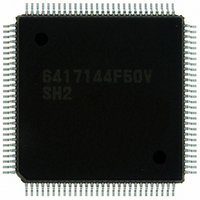
HD6417144F50V Renesas Electronics America, HD6417144F50V Datasheet - Page 29

HD6417144F50V
Manufacturer Part Number
HD6417144F50V
Description
IC SUPERH MCU ROMLESS 112QFP
Manufacturer
Renesas Electronics America
Series
SuperH® SH7144r
Datasheet
1.HD64F7144F50V.pdf
(932 pages)
Specifications of HD6417144F50V
Core Processor
SH-2
Core Size
32-Bit
Speed
50MHz
Connectivity
EBI/EMI, I²C, SCI
Peripherals
DMA, POR, PWM, WDT
Number Of I /o
74
Program Memory Type
ROMless
Ram Size
8K x 8
Voltage - Supply (vcc/vdd)
3 V ~ 3.6 V
Data Converters
A/D 8x10b
Oscillator Type
Internal
Operating Temperature
-20°C ~ 75°C
Package / Case
112-QFP
For Use With
HS0005KCU11H - EMULATOR E10A-USB H8S(X),SH2(A)EDK7145 - DEV EVALUATION KIT SH7145
Lead Free Status / RoHS Status
Lead free / RoHS Compliant
Eeprom Size
-
Program Memory Size
-
Available stocks
Company
Part Number
Manufacturer
Quantity
Price
Company:
Part Number:
HD6417144F50V
Manufacturer:
Renesas Electronics America
Quantity:
10 000
- Current page: 29 of 932
- Download datasheet (6Mb)
Figure 10.11 DMA Transfer Example in Cycle-Steal Mode ......................................................195
Figure 10.12 DMA Transfer Example in Burst Mode ................................................................195
Figure 10.13 Bus Handling when Multiple Channels Are Operating .........................................197
Figure 10.14 Cycle Steal, Dual Address and Level Detection (Fastest Operation) ....................200
Figure 10.15 Cycle Steal, Dual Address and Level Detection (Normal Operation) ...................200
Figure 10.16 Cycle Steal, Single Address and Level Detection (Fastest Operation)..................200
Figure 10.17 Cycle Steal, Single Address and Level Detection (Normal Operation).................200
Figure 10.18 Burst Mode, Dual Address and Level Detection (Fastest Operation)....................201
Figure 10.19 Burst Mode, Dual Address and Level Detection (Normal Operation)...................201
Figure 10.20 Burst Mode, Single Address and Level Detection (Fastest Operation) .................201
Figure 10.21 Burst Mode, Single Address and Level Detection (Normal Operation) ................202
Figure 10.22 Burst Mode, Dual Address and Edge Detection ....................................................202
Figure 10.23 Burst Mode, Single Address and Edge Detection..................................................202
Figure 10.24 Source Address Reload Function...........................................................................203
Figure 10.25 Source Address Reload Function Timing Chart ....................................................203
Section 11 Multi-Function Timer Pulse Unit (MTU)
Figure 11.1 Block Diagram of MTU ..........................................................................................216
Figure 11.2 Complementary PWM Mode Output Level Example .............................................254
Figure 11.3 Example of Counter Operation Setting Procedure ..................................................259
Figure 11.4 Free-Running Counter Operation ............................................................................260
Figure 11.5 Periodic Counter Operation .....................................................................................261
Figure 11.6 Example of Setting Procedure for Waveform Output by Compare Match ..............261
Figure 11.7 Example of 0 Output/1 Output Operation................................................................262
Figure 11.8 Example of Toggle Output Operation .....................................................................262
Figure 11.9 Example of Input Capture Operation Setting Procedure .........................................263
Figure 11.10 Example of Input Capture Operation.....................................................................264
Figure 11.11 Example of Synchronous Operation Setting Procedure.........................................265
Figure 11.12 Example of Synchronous Operation......................................................................266
Figure 11.13 Compare Match Buffer Operation .........................................................................267
Figure 11.14 Input Capture Buffer Operation.............................................................................267
Figure 11.15 Example of Buffer Operation Setting Procedure ...................................................267
Figure 11.16 Example of Buffer Operation (1)...........................................................................268
Figure 11.17 Example of Buffer Operation (2)...........................................................................269
Figure 11.18 Cascaded Operation Setting Procedure .................................................................270
Figure 11.19 Example of Cascaded Operation ...........................................................................270
Figure 11.20 Example of PWM Mode Setting Procedure ..........................................................273
Figure 11.21 Example of PWM Mode Operation (1) .................................................................273
Figure 11.22 Example of PWM Mode Operation (2) .................................................................274
Figure 11.23 Example of PWM Mode Operation (3) .................................................................275
Figure 11.24 Example of Phase Counting Mode Setting Procedure...........................................276
Rev.4.00 Mar. 27, 2008, Page xxvii of xliv
REJ09B0108-0400
Related parts for HD6417144F50V
Image
Part Number
Description
Manufacturer
Datasheet
Request
R

Part Number:
Description:
KIT STARTER FOR M16C/29
Manufacturer:
Renesas Electronics America
Datasheet:

Part Number:
Description:
KIT STARTER FOR R8C/2D
Manufacturer:
Renesas Electronics America
Datasheet:

Part Number:
Description:
R0K33062P STARTER KIT
Manufacturer:
Renesas Electronics America
Datasheet:

Part Number:
Description:
KIT STARTER FOR R8C/23 E8A
Manufacturer:
Renesas Electronics America
Datasheet:

Part Number:
Description:
KIT STARTER FOR R8C/25
Manufacturer:
Renesas Electronics America
Datasheet:

Part Number:
Description:
KIT STARTER H8S2456 SHARPE DSPLY
Manufacturer:
Renesas Electronics America
Datasheet:

Part Number:
Description:
KIT STARTER FOR R8C38C
Manufacturer:
Renesas Electronics America
Datasheet:

Part Number:
Description:
KIT STARTER FOR R8C35C
Manufacturer:
Renesas Electronics America
Datasheet:

Part Number:
Description:
KIT STARTER FOR R8CL3AC+LCD APPS
Manufacturer:
Renesas Electronics America
Datasheet:

Part Number:
Description:
KIT STARTER FOR RX610
Manufacturer:
Renesas Electronics America
Datasheet:

Part Number:
Description:
KIT STARTER FOR R32C/118
Manufacturer:
Renesas Electronics America
Datasheet:

Part Number:
Description:
KIT DEV RSK-R8C/26-29
Manufacturer:
Renesas Electronics America
Datasheet:

Part Number:
Description:
KIT STARTER FOR SH7124
Manufacturer:
Renesas Electronics America
Datasheet:

Part Number:
Description:
KIT STARTER FOR H8SX/1622
Manufacturer:
Renesas Electronics America
Datasheet:

Part Number:
Description:
KIT DEV FOR SH7203
Manufacturer:
Renesas Electronics America
Datasheet:


