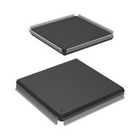
HD6417727F100CV Renesas Electronics America, HD6417727F100CV Datasheet - Page 131

HD6417727F100CV
Manufacturer Part Number
HD6417727F100CV
Description
SH3-DSP, LEAD FREE
Manufacturer
Renesas Electronics America
Series
SuperH® SH7700r
Datasheet
1.HD6417727BP100CV.pdf
(1098 pages)
Specifications of HD6417727F100CV
Core Processor
SH-3 DSP
Core Size
32-Bit
Speed
100MHz
Connectivity
FIFO, SCI, SIO, SmartCard, USB
Peripherals
DMA, LCD, POR, WDT
Number Of I /o
104
Program Memory Type
ROMless
Ram Size
32K x 8
Voltage - Supply (vcc/vdd)
1.6 V ~ 2.05 V
Data Converters
A/D 6x10b; D/A 2x8b
Oscillator Type
Internal
Operating Temperature
-20°C ~ 75°C
Package / Case
240-QFP Exposed Pad, 240-eQFP, 240-HQFP
Cpu Family
SuperH
Device Core Size
32b
Frequency (max)
100MHz
Interface Type
SCI/USB
Program Memory Size
Not Required
Total Internal Ram Size
16KB
# I/os (max)
104
Number Of Timers - General Purpose
4
Operating Supply Voltage (typ)
1.8/3.3V
Operating Supply Voltage (max)
2.05/3.6V
Operating Supply Voltage (min)
1.6/2.6V
On-chip Adc
6-chx10-bit
On-chip Dac
2-chx8-bit
Instruction Set Architecture
RISC
Operating Temp Range
-20C to 75C
Operating Temperature Classification
Commercial
Mounting
Surface Mount
Pin Count
240
Package Type
HQFP
Lead Free Status / RoHS Status
Lead free / RoHS Compliant
Eeprom Size
-
Program Memory Size
-
Lead Free Status / Rohs Status
Compliant
- Current page: 131 of 1098
- Download datasheet (7Mb)
Notes: 1. The normal minimum number of execution cycles is two, but five cycles are required
Logic Operation Instructions
Table 2.22 Logic Operation Instructions
Instruction
AND
AND
AND.B #imm,@(R0,GBR)
NOT
OR
OR
OR.B
TAS.B @Rn*
TST
TST
TST.B #imm,@(R0,GBR)
XOR
XOR
XOR.B #imm,@(R0,GBR)
Note:
Rm,Rn
#imm,R0
Rm,Rn
Rm,Rn
#imm,R0
#imm,@(R0,GBR)
Rm,Rn
#imm,R0
Rm,Rn
#imm,R0
2. The normal minimum number of execution cycles is one, but three cycles are required
*
when the operation result is read from the MAC register immediately after the
instruction.
when the operation result is read from the MAC register immediately after the MUL
instruction.
An on-chip DMAC bus cycle is not inserted between a TAS instruction operand read
cycle and write cycle. Also, bus release is not performed by BREQ.
Operation
Rn & Rm → Rn
R0 & imm → R0
(R0 + GBR) & imm →
(R0 + GBR)
~Rm → Rn
Rn | Rm → Rn
R0 | imm → R0
(R0 + GBR) | imm →
(R0 + GBR)
If (Rn) is 0, 1 → T;
1 → MSB of (Rn)
Rn & Rm; if the result
is 0, 1 → T
R0 & imm; if the result
is 0, 1 → T
(R0 + GBR) & imm;
if the result is 0, 1 → T
Rn ^ Rm → Rn
R0 ^ imm → R0
(R0 + GBR) ^ imm →
(R0 + GBR)
Code
0010nnnnmmmm1001
11001001iiiiiiii
11001101iiiiiiii
0110nnnnmmmm0111
0010nnnnmmmm1011
11001011iiiiiiii
11001111iiiiiiii
0100nnnn00011011
0010nnnnmmmm1000
11001000iiiiiiii
11001100iiiiiiii
0010nnnnmmmm1010
11001010iiiiiiii
11001110iiiiiiii
Rev.6.00 Mar. 27, 2009 Page 73 of 1036
Privileged
Mode
—
—
—
—
—
—
—
—
—
—
—
—
—
—
REJ09B0254-0600
Section 2 CPU
Cycles T Bit
1
1
3
1
1
1
3
4
1
1
3
1
1
3
—
—
—
—
—
—
—
Test
result
Test
result
Test
result
Test
result
—
—
—
Related parts for HD6417727F100CV
Image
Part Number
Description
Manufacturer
Datasheet
Request
R

Part Number:
Description:
KIT STARTER FOR M16C/29
Manufacturer:
Renesas Electronics America
Datasheet:

Part Number:
Description:
KIT STARTER FOR R8C/2D
Manufacturer:
Renesas Electronics America
Datasheet:

Part Number:
Description:
R0K33062P STARTER KIT
Manufacturer:
Renesas Electronics America
Datasheet:

Part Number:
Description:
KIT STARTER FOR R8C/23 E8A
Manufacturer:
Renesas Electronics America
Datasheet:

Part Number:
Description:
KIT STARTER FOR R8C/25
Manufacturer:
Renesas Electronics America
Datasheet:

Part Number:
Description:
KIT STARTER H8S2456 SHARPE DSPLY
Manufacturer:
Renesas Electronics America
Datasheet:

Part Number:
Description:
KIT STARTER FOR R8C38C
Manufacturer:
Renesas Electronics America
Datasheet:

Part Number:
Description:
KIT STARTER FOR R8C35C
Manufacturer:
Renesas Electronics America
Datasheet:

Part Number:
Description:
KIT STARTER FOR R8CL3AC+LCD APPS
Manufacturer:
Renesas Electronics America
Datasheet:

Part Number:
Description:
KIT STARTER FOR RX610
Manufacturer:
Renesas Electronics America
Datasheet:

Part Number:
Description:
KIT STARTER FOR R32C/118
Manufacturer:
Renesas Electronics America
Datasheet:

Part Number:
Description:
KIT DEV RSK-R8C/26-29
Manufacturer:
Renesas Electronics America
Datasheet:

Part Number:
Description:
KIT STARTER FOR SH7124
Manufacturer:
Renesas Electronics America
Datasheet:

Part Number:
Description:
KIT STARTER FOR H8SX/1622
Manufacturer:
Renesas Electronics America
Datasheet:

Part Number:
Description:
KIT DEV FOR SH7203
Manufacturer:
Renesas Electronics America
Datasheet:


