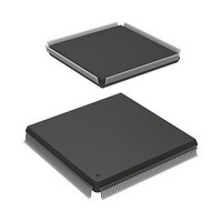
HD6417727F100CV Renesas Electronics America, HD6417727F100CV Datasheet - Page 183

HD6417727F100CV
Manufacturer Part Number
HD6417727F100CV
Description
SH3-DSP, LEAD FREE
Manufacturer
Renesas Electronics America
Series
SuperH® SH7700r
Datasheet
1.HD6417727BP100CV.pdf
(1098 pages)
Specifications of HD6417727F100CV
Core Processor
SH-3 DSP
Core Size
32-Bit
Speed
100MHz
Connectivity
FIFO, SCI, SIO, SmartCard, USB
Peripherals
DMA, LCD, POR, WDT
Number Of I /o
104
Program Memory Type
ROMless
Ram Size
32K x 8
Voltage - Supply (vcc/vdd)
1.6 V ~ 2.05 V
Data Converters
A/D 6x10b; D/A 2x8b
Oscillator Type
Internal
Operating Temperature
-20°C ~ 75°C
Package / Case
240-QFP Exposed Pad, 240-eQFP, 240-HQFP
Cpu Family
SuperH
Device Core Size
32b
Frequency (max)
100MHz
Interface Type
SCI/USB
Program Memory Size
Not Required
Total Internal Ram Size
16KB
# I/os (max)
104
Number Of Timers - General Purpose
4
Operating Supply Voltage (typ)
1.8/3.3V
Operating Supply Voltage (max)
2.05/3.6V
Operating Supply Voltage (min)
1.6/2.6V
On-chip Adc
6-chx10-bit
On-chip Dac
2-chx8-bit
Instruction Set Architecture
RISC
Operating Temp Range
-20C to 75C
Operating Temperature Classification
Commercial
Mounting
Surface Mount
Pin Count
240
Package Type
HQFP
Lead Free Status / RoHS Status
Lead free / RoHS Compliant
Eeprom Size
-
Program Memory Size
-
Lead Free Status / Rohs Status
Compliant
- Current page: 183 of 1098
- Download datasheet (7Mb)
3.6.1
The address array is assigned to H'F2000000 to H'F2FFFFFF. To access an address array, the
32-bit address field (for read/write operations) and 32-bit data field (for write operations) must be
specified. The address field specifies information for selecting the entry to be accessed; the data
field specifies the VPN, V bit and ASID to be written to the address array ((1) in figure 3.15).
In the address field, specify VPN (16 to 12) as the index address for selecting the entry (bits 16 to
12), the W bits for selecting the way (bits 9 and 8), and H'F2 to indicate address array access (bits
31 to 24). The IX bit in MMUCR indicates whether an EX-OR of VPN (16 to 12) and ASID (4 to
0) in the PTEH register is taken as the index address.
When writing, the write is performed to the entry selected with the index address and way.
When reading, the VPN, V bit, and ASID of the entry selected with the index address and way in
the format of the data field in figure 3.12 without comparing addresses. 0 is written to data field
bits 16 to 12.
To invalidate a specific entry, specify the entry and way, and write 0 to the corresponding V bit.
3.6.2
The data array is assigned to H'F3000000 to H'F3FFFFFF. To access a data array, the 32-bit
address field (for read/write operations), and 32-bit data field (for write operations) must be
specified. The address section specifies information for selecting the entry to be accessed; the data
section specifies the longword data to be written to the data array ((2) in figure 3.15). Longword
data has the same bit configuration as PTEL.
In the address field, specify VPN (16 to 12) as the index address for selecting the entry (bits 16 to
12), the W bits for selecting the way (bits 9 and 8), and H'F3 to indicate data array access (bits 31
to 24). The IX bit in MMUCR indicates whether an EX-OR of VPN (16 to 12) and ASID (4 to 0)
in the PTEH register is taken as the index address.
Both reading and writing use the longword of the data array specified by the entry address and
way number.
Address Array
Data Array
Section 3 Memory Management Unit (MMU)
Rev.6.00 Mar. 27, 2009 Page 125 of 1036
REJ09B0254-0600
Related parts for HD6417727F100CV
Image
Part Number
Description
Manufacturer
Datasheet
Request
R

Part Number:
Description:
KIT STARTER FOR M16C/29
Manufacturer:
Renesas Electronics America
Datasheet:

Part Number:
Description:
KIT STARTER FOR R8C/2D
Manufacturer:
Renesas Electronics America
Datasheet:

Part Number:
Description:
R0K33062P STARTER KIT
Manufacturer:
Renesas Electronics America
Datasheet:

Part Number:
Description:
KIT STARTER FOR R8C/23 E8A
Manufacturer:
Renesas Electronics America
Datasheet:

Part Number:
Description:
KIT STARTER FOR R8C/25
Manufacturer:
Renesas Electronics America
Datasheet:

Part Number:
Description:
KIT STARTER H8S2456 SHARPE DSPLY
Manufacturer:
Renesas Electronics America
Datasheet:

Part Number:
Description:
KIT STARTER FOR R8C38C
Manufacturer:
Renesas Electronics America
Datasheet:

Part Number:
Description:
KIT STARTER FOR R8C35C
Manufacturer:
Renesas Electronics America
Datasheet:

Part Number:
Description:
KIT STARTER FOR R8CL3AC+LCD APPS
Manufacturer:
Renesas Electronics America
Datasheet:

Part Number:
Description:
KIT STARTER FOR RX610
Manufacturer:
Renesas Electronics America
Datasheet:

Part Number:
Description:
KIT STARTER FOR R32C/118
Manufacturer:
Renesas Electronics America
Datasheet:

Part Number:
Description:
KIT DEV RSK-R8C/26-29
Manufacturer:
Renesas Electronics America
Datasheet:

Part Number:
Description:
KIT STARTER FOR SH7124
Manufacturer:
Renesas Electronics America
Datasheet:

Part Number:
Description:
KIT STARTER FOR H8SX/1622
Manufacturer:
Renesas Electronics America
Datasheet:

Part Number:
Description:
KIT DEV FOR SH7203
Manufacturer:
Renesas Electronics America
Datasheet:


