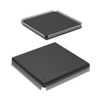
HD6417727F100CV Renesas Electronics America, HD6417727F100CV Datasheet - Page 650

HD6417727F100CV
Manufacturer Part Number
HD6417727F100CV
Description
SH3-DSP, LEAD FREE
Manufacturer
Renesas Electronics America
Series
SuperH® SH7700r
Datasheet
1.HD6417727BP100CV.pdf
(1098 pages)
Specifications of HD6417727F100CV
Core Processor
SH-3 DSP
Core Size
32-Bit
Speed
100MHz
Connectivity
FIFO, SCI, SIO, SmartCard, USB
Peripherals
DMA, LCD, POR, WDT
Number Of I /o
104
Program Memory Type
ROMless
Ram Size
32K x 8
Voltage - Supply (vcc/vdd)
1.6 V ~ 2.05 V
Data Converters
A/D 6x10b; D/A 2x8b
Oscillator Type
Internal
Operating Temperature
-20°C ~ 75°C
Package / Case
240-QFP Exposed Pad, 240-eQFP, 240-HQFP
Cpu Family
SuperH
Device Core Size
32b
Frequency (max)
100MHz
Interface Type
SCI/USB
Program Memory Size
Not Required
Total Internal Ram Size
16KB
# I/os (max)
104
Number Of Timers - General Purpose
4
Operating Supply Voltage (typ)
1.8/3.3V
Operating Supply Voltage (max)
2.05/3.6V
Operating Supply Voltage (min)
1.6/2.6V
On-chip Adc
6-chx10-bit
On-chip Dac
2-chx8-bit
Instruction Set Architecture
RISC
Operating Temp Range
-20C to 75C
Operating Temperature Classification
Commercial
Mounting
Surface Mount
Pin Count
240
Package Type
HQFP
Lead Free Status / RoHS Status
Lead free / RoHS Compliant
Eeprom Size
-
Program Memory Size
-
Lead Free Status / Rohs Status
Compliant
- Current page: 650 of 1098
- Download datasheet (7Mb)
Section 19 Serial Communication Interface with FIFO (SCIF)
Figure 19.4 is a sample flowchart for initializing the SCIF. The procedure for initializing the SCIF
is:
Rev.6.00 Mar. 27, 2009 Page 592 of 1036
REJ09B0254-0600
Clear TE and RE bits in SCSCR2 to 0
bits in SCSCR2 (leaving TE and RE
Set data transfer format in SCSMR2
Set RTRG1-0, TTRG1-0, and MCE
Clear TFRST and RFRST bits to 0
Set TFRST and RFRST bits in
SCSCR2 to 1,and set RIE,
Set TE and RE bits in
1-bit interval elapsed?
Set CKE1 and CKE0
Set value in SCBRR2
bits cleared to 0)
SCFCR2 to 1
and TIE bits
Initialization
in SCFCR2
End
Figure 19.4 Sample SCIF Initialization Flowchart
Yes
Wait
(4)
No
(1)
(2)
(3)
(1) Set the clock selection in SCSCR2.
(2) Set the data transfer format in SCSMR2.
(3) Write a value corresponding to the bit rate
(4) Wait at least one bit interval, then set the
Be sure to clear bits RIE TIE, TE, and RE
to 0.
When clock output is selected, it is output
immediately after SCSCR2 settings are made.
into the bit rate register 2 (SCBRR2).
(Not necessary if an external clock is used.)
TE bit or RE bit in SCSR2 to 1. Also set the
RIE and TIE bits.
Setting the TE and RE bits enables the
TxD2 and RxD2 pins to be used. When
transmitting, the SCIF will go to the mark
state; when receiving, it will go to the idle
state, waiting for a start bit.
Related parts for HD6417727F100CV
Image
Part Number
Description
Manufacturer
Datasheet
Request
R

Part Number:
Description:
KIT STARTER FOR M16C/29
Manufacturer:
Renesas Electronics America
Datasheet:

Part Number:
Description:
KIT STARTER FOR R8C/2D
Manufacturer:
Renesas Electronics America
Datasheet:

Part Number:
Description:
R0K33062P STARTER KIT
Manufacturer:
Renesas Electronics America
Datasheet:

Part Number:
Description:
KIT STARTER FOR R8C/23 E8A
Manufacturer:
Renesas Electronics America
Datasheet:

Part Number:
Description:
KIT STARTER FOR R8C/25
Manufacturer:
Renesas Electronics America
Datasheet:

Part Number:
Description:
KIT STARTER H8S2456 SHARPE DSPLY
Manufacturer:
Renesas Electronics America
Datasheet:

Part Number:
Description:
KIT STARTER FOR R8C38C
Manufacturer:
Renesas Electronics America
Datasheet:

Part Number:
Description:
KIT STARTER FOR R8C35C
Manufacturer:
Renesas Electronics America
Datasheet:

Part Number:
Description:
KIT STARTER FOR R8CL3AC+LCD APPS
Manufacturer:
Renesas Electronics America
Datasheet:

Part Number:
Description:
KIT STARTER FOR RX610
Manufacturer:
Renesas Electronics America
Datasheet:

Part Number:
Description:
KIT STARTER FOR R32C/118
Manufacturer:
Renesas Electronics America
Datasheet:

Part Number:
Description:
KIT DEV RSK-R8C/26-29
Manufacturer:
Renesas Electronics America
Datasheet:

Part Number:
Description:
KIT STARTER FOR SH7124
Manufacturer:
Renesas Electronics America
Datasheet:

Part Number:
Description:
KIT STARTER FOR H8SX/1622
Manufacturer:
Renesas Electronics America
Datasheet:

Part Number:
Description:
KIT DEV FOR SH7203
Manufacturer:
Renesas Electronics America
Datasheet:


