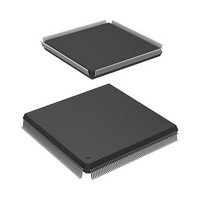
HD6417727F100CV Renesas Electronics America, HD6417727F100CV Datasheet - Page 62

HD6417727F100CV
Manufacturer Part Number
HD6417727F100CV
Description
SH3-DSP, LEAD FREE
Manufacturer
Renesas Electronics America
Series
SuperH® SH7700r
Datasheet
1.HD6417727BP100CV.pdf
(1098 pages)
Specifications of HD6417727F100CV
Core Processor
SH-3 DSP
Core Size
32-Bit
Speed
100MHz
Connectivity
FIFO, SCI, SIO, SmartCard, USB
Peripherals
DMA, LCD, POR, WDT
Number Of I /o
104
Program Memory Type
ROMless
Ram Size
32K x 8
Voltage - Supply (vcc/vdd)
1.6 V ~ 2.05 V
Data Converters
A/D 6x10b; D/A 2x8b
Oscillator Type
Internal
Operating Temperature
-20°C ~ 75°C
Package / Case
240-QFP Exposed Pad, 240-eQFP, 240-HQFP
Cpu Family
SuperH
Device Core Size
32b
Frequency (max)
100MHz
Interface Type
SCI/USB
Program Memory Size
Not Required
Total Internal Ram Size
16KB
# I/os (max)
104
Number Of Timers - General Purpose
4
Operating Supply Voltage (typ)
1.8/3.3V
Operating Supply Voltage (max)
2.05/3.6V
Operating Supply Voltage (min)
1.6/2.6V
On-chip Adc
6-chx10-bit
On-chip Dac
2-chx8-bit
Instruction Set Architecture
RISC
Operating Temp Range
-20C to 75C
Operating Temperature Classification
Commercial
Mounting
Surface Mount
Pin Count
240
Package Type
HQFP
Lead Free Status / RoHS Status
Lead free / RoHS Compliant
Eeprom Size
-
Program Memory Size
-
Lead Free Status / Rohs Status
Compliant
- Current page: 62 of 1098
- Download datasheet (7Mb)
Section 1 Overview and Pin Functions
Item
Memory
management
unit (MMU)
Cache memory
X/Y memory
Interrupt
controller (INTC)
User break
controller (UBC)
Rev.6.00 Mar. 27, 2009 Page 4 of 1036
REJ09B0254-0600
Features
•
•
•
•
•
•
•
•
•
•
•
•
•
•
•
•
•
•
•
4 Gbytes of address space, 256 address spaces (ASID 8 bits)
Page unit sharing
Supports multiple page sizes: 1 kbytes or 4 kbytes
128-entry, 4-way set associative TLB
Supports software selection of replacement method and random-
replacement algorithms
Contents of TLB can directly be accessed according to the address mapping
16-kbyte cache, mixed instruction/data
256 entries, 4-way set associative, 16-byte block length
Write-back, write-through, least recently used (LRU) replacement algorithm
1-stage write-back buffer
Maximum 2 ways of the cache can be locked
User-selectable mapping mechanism
⎯ Fixed mapping for mission-critical realtime applications
⎯ Automatic mapping through TLB for easy to use
3 independent read/write ports
⎯ 8-/16-/32-bit access from the CPU
⎯ Maximum two 16-bit accesses from the DSP
⎯ 8-/16-/32-bit access from the DMAC
8-kbyte RAM for X and Y memory individually
7 external interrupt pins (NMI, IRQ5–IRQ0)
On-chip peripheral interrupts: set priority levels for each module
2 break channels
Addresses, data values, type of access, and data size can all be set as
break conditions
Supports a sequential break function
Related parts for HD6417727F100CV
Image
Part Number
Description
Manufacturer
Datasheet
Request
R

Part Number:
Description:
KIT STARTER FOR M16C/29
Manufacturer:
Renesas Electronics America
Datasheet:

Part Number:
Description:
KIT STARTER FOR R8C/2D
Manufacturer:
Renesas Electronics America
Datasheet:

Part Number:
Description:
R0K33062P STARTER KIT
Manufacturer:
Renesas Electronics America
Datasheet:

Part Number:
Description:
KIT STARTER FOR R8C/23 E8A
Manufacturer:
Renesas Electronics America
Datasheet:

Part Number:
Description:
KIT STARTER FOR R8C/25
Manufacturer:
Renesas Electronics America
Datasheet:

Part Number:
Description:
KIT STARTER H8S2456 SHARPE DSPLY
Manufacturer:
Renesas Electronics America
Datasheet:

Part Number:
Description:
KIT STARTER FOR R8C38C
Manufacturer:
Renesas Electronics America
Datasheet:

Part Number:
Description:
KIT STARTER FOR R8C35C
Manufacturer:
Renesas Electronics America
Datasheet:

Part Number:
Description:
KIT STARTER FOR R8CL3AC+LCD APPS
Manufacturer:
Renesas Electronics America
Datasheet:

Part Number:
Description:
KIT STARTER FOR RX610
Manufacturer:
Renesas Electronics America
Datasheet:

Part Number:
Description:
KIT STARTER FOR R32C/118
Manufacturer:
Renesas Electronics America
Datasheet:

Part Number:
Description:
KIT DEV RSK-R8C/26-29
Manufacturer:
Renesas Electronics America
Datasheet:

Part Number:
Description:
KIT STARTER FOR SH7124
Manufacturer:
Renesas Electronics America
Datasheet:

Part Number:
Description:
KIT STARTER FOR H8SX/1622
Manufacturer:
Renesas Electronics America
Datasheet:

Part Number:
Description:
KIT DEV FOR SH7203
Manufacturer:
Renesas Electronics America
Datasheet:


