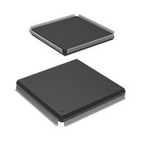
HD6417727F100CV Renesas Electronics America, HD6417727F100CV Datasheet - Page 63

HD6417727F100CV
Manufacturer Part Number
HD6417727F100CV
Description
SH3-DSP, LEAD FREE
Manufacturer
Renesas Electronics America
Series
SuperH® SH7700r
Datasheet
1.HD6417727BP100CV.pdf
(1098 pages)
Specifications of HD6417727F100CV
Core Processor
SH-3 DSP
Core Size
32-Bit
Speed
100MHz
Connectivity
FIFO, SCI, SIO, SmartCard, USB
Peripherals
DMA, LCD, POR, WDT
Number Of I /o
104
Program Memory Type
ROMless
Ram Size
32K x 8
Voltage - Supply (vcc/vdd)
1.6 V ~ 2.05 V
Data Converters
A/D 6x10b; D/A 2x8b
Oscillator Type
Internal
Operating Temperature
-20°C ~ 75°C
Package / Case
240-QFP Exposed Pad, 240-eQFP, 240-HQFP
Cpu Family
SuperH
Device Core Size
32b
Frequency (max)
100MHz
Interface Type
SCI/USB
Program Memory Size
Not Required
Total Internal Ram Size
16KB
# I/os (max)
104
Number Of Timers - General Purpose
4
Operating Supply Voltage (typ)
1.8/3.3V
Operating Supply Voltage (max)
2.05/3.6V
Operating Supply Voltage (min)
1.6/2.6V
On-chip Adc
6-chx10-bit
On-chip Dac
2-chx8-bit
Instruction Set Architecture
RISC
Operating Temp Range
-20C to 75C
Operating Temperature Classification
Commercial
Mounting
Surface Mount
Pin Count
240
Package Type
HQFP
Lead Free Status / RoHS Status
Lead free / RoHS Compliant
Eeprom Size
-
Program Memory Size
-
Lead Free Status / Rohs Status
Compliant
- Current page: 63 of 1098
- Download datasheet (7Mb)
Item
Bus state
controller (BSC)
Li bus state
controller (LBSC)
User debug
Interface (H-UDI)
Timer (TMU)
Realtime clock
(RTC)
Serial communi-
cation interface
(SCI)
Features
•
•
•
•
•
•
•
•
•
•
•
•
•
•
•
•
•
•
Physical address space divided into six areas (area 0, areas 2 to 6), each of
up to 64 Mbytes, with the following features settable for each area:
⎯ Bus size (8, 16, or 32 bits)
⎯ Number of wait cycles (hardware wait function also waited)
⎯ Direct connection of SRAM, synchronous DRAM, and burst ROM
⎯ Supports PCMCIA interface (2 channels)
⎯ Chip select signals (CS0, CS2–CS6) for relevant area
Synchronous DRAM refresh function
⎯ Programmable refresh interval
⎯ Supports CAS-before-RAS refresh and self-refresh modes
⎯ Supports power-down DRAM
Synchronous DRAM burst access function
Big endian or little endian can be specified
Bus State Controller for LCDC or USB Host
Supports synchronous DRAM
Synchronous DRAM access function (area 3)
E10A emulator support
Pin arrangement conforming to JTAG specification
Realtime branch trace
3-channel auto-reload-type 32-bit timer
Choice of six counter input clocks
Maximum resolution: 2 MHz
Built-in clock, calendar functions, and alarm functions
On-chip 32-kHz crystal oscillator circuit with a maximum resolution (cycle
interrupt) of 1/256 second
Asynchronous mode or clock synchronous mode can be selected
Full-duplex communication
Supports smart card interface
possible by designating memory to be connected to each area
Rev.6.00 Mar. 27, 2009 Page 5 of 1036
Section 1 Overview and Pin Functions
REJ09B0254-0600
Related parts for HD6417727F100CV
Image
Part Number
Description
Manufacturer
Datasheet
Request
R

Part Number:
Description:
KIT STARTER FOR M16C/29
Manufacturer:
Renesas Electronics America
Datasheet:

Part Number:
Description:
KIT STARTER FOR R8C/2D
Manufacturer:
Renesas Electronics America
Datasheet:

Part Number:
Description:
R0K33062P STARTER KIT
Manufacturer:
Renesas Electronics America
Datasheet:

Part Number:
Description:
KIT STARTER FOR R8C/23 E8A
Manufacturer:
Renesas Electronics America
Datasheet:

Part Number:
Description:
KIT STARTER FOR R8C/25
Manufacturer:
Renesas Electronics America
Datasheet:

Part Number:
Description:
KIT STARTER H8S2456 SHARPE DSPLY
Manufacturer:
Renesas Electronics America
Datasheet:

Part Number:
Description:
KIT STARTER FOR R8C38C
Manufacturer:
Renesas Electronics America
Datasheet:

Part Number:
Description:
KIT STARTER FOR R8C35C
Manufacturer:
Renesas Electronics America
Datasheet:

Part Number:
Description:
KIT STARTER FOR R8CL3AC+LCD APPS
Manufacturer:
Renesas Electronics America
Datasheet:

Part Number:
Description:
KIT STARTER FOR RX610
Manufacturer:
Renesas Electronics America
Datasheet:

Part Number:
Description:
KIT STARTER FOR R32C/118
Manufacturer:
Renesas Electronics America
Datasheet:

Part Number:
Description:
KIT DEV RSK-R8C/26-29
Manufacturer:
Renesas Electronics America
Datasheet:

Part Number:
Description:
KIT STARTER FOR SH7124
Manufacturer:
Renesas Electronics America
Datasheet:

Part Number:
Description:
KIT STARTER FOR H8SX/1622
Manufacturer:
Renesas Electronics America
Datasheet:

Part Number:
Description:
KIT DEV FOR SH7203
Manufacturer:
Renesas Electronics America
Datasheet:


