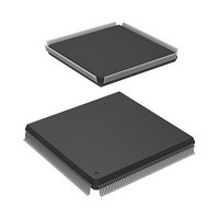
HD6417727F100CV Renesas Electronics America, HD6417727F100CV Datasheet - Page 891

HD6417727F100CV
Manufacturer Part Number
HD6417727F100CV
Description
SH3-DSP, LEAD FREE
Manufacturer
Renesas Electronics America
Series
SuperH® SH7700r
Datasheet
1.HD6417727BP100CV.pdf
(1098 pages)
Specifications of HD6417727F100CV
Core Processor
SH-3 DSP
Core Size
32-Bit
Speed
100MHz
Connectivity
FIFO, SCI, SIO, SmartCard, USB
Peripherals
DMA, LCD, POR, WDT
Number Of I /o
104
Program Memory Type
ROMless
Ram Size
32K x 8
Voltage - Supply (vcc/vdd)
1.6 V ~ 2.05 V
Data Converters
A/D 6x10b; D/A 2x8b
Oscillator Type
Internal
Operating Temperature
-20°C ~ 75°C
Package / Case
240-QFP Exposed Pad, 240-eQFP, 240-HQFP
Cpu Family
SuperH
Device Core Size
32b
Frequency (max)
100MHz
Interface Type
SCI/USB
Program Memory Size
Not Required
Total Internal Ram Size
16KB
# I/os (max)
104
Number Of Timers - General Purpose
4
Operating Supply Voltage (typ)
1.8/3.3V
Operating Supply Voltage (max)
2.05/3.6V
Operating Supply Voltage (min)
1.6/2.6V
On-chip Adc
6-chx10-bit
On-chip Dac
2-chx8-bit
Instruction Set Architecture
RISC
Operating Temp Range
-20C to 75C
Operating Temperature Classification
Commercial
Mounting
Surface Mount
Pin Count
240
Package Type
HQFP
Lead Free Status / RoHS Status
Lead free / RoHS Compliant
Eeprom Size
-
Program Memory Size
-
Lead Free Status / Rohs Status
Compliant
- Current page: 891 of 1098
- Download datasheet (7Mb)
26.3.7
For details on using versions previous to the SH7727B please refer to appendix F, Specifications
for Using Port G Control Register (PGCR) with Versions Previous to the SH7727B.
Port G Control Register (PGCR) is a 16-bit read/write register that selects the pin functions.
PGCR is initialized to H'AAAA (ASEMD0 = 1) or H'A200 (ASEMD0 = 0) by power-on resets;
however, it is not initialized by manual resets, in standby mode, or in sleep mode.
Bits 15, 14: PG7 Mode 1, 0 (PG7MD1, PG7MD0)
Bits 13, 12: Reserved
Bits 11, 10: PG5 Mode 1, 0 (PG5MD1, PG5MD0)
Bits 9, 8: PG4 Mode 1, 0 (PG4MD1, PG4MD0)
Bits 7, 6: PG3 Mode 1, 0 (PG3MD1, PG3MD0)
Bits 5, 4: PG2 Mode 1, 0 (PG2MD1, PG2MD0)
Bits 3, 2: PG1 Mode 1, 0 (PG1MD1, PG1MD0)
Bits 1, 0: PG0 Mode 1, 0 (PG0MD1, PG0MD0)
These bits select the pin functions and the input pullup MOS control.
Initial value:
R/W: R/W R/W
Bit:
Port G Control Register (PGCR)
PG7
MD1
15
1
MD0
PG7
14
0
13
⎯
R
1
12
⎯
R
0
PG5
MD1
R/W R/W R/W R/W R/W R/W R/W R/W R/W R/W R/W R/W
1/0
11
PG5
MD0
10
0
MD1
PG4
9
1
PG4
MD0
8
0
Rev.6.00 Mar. 27, 2009 Page 833 of 1036
MD1
PG3
1/0
Section 26 Pin Function Controller (PFC)
7
MD0
PG3
6
0
MD1
PG2
1/0
5
MD0
PG2
4
0
MD1
PG1
1/0
3
REJ09B0254-0600
MD0
PG1
2
0
MD1
PG0
1/0
1
MD0
PG0
0
0
Related parts for HD6417727F100CV
Image
Part Number
Description
Manufacturer
Datasheet
Request
R

Part Number:
Description:
KIT STARTER FOR M16C/29
Manufacturer:
Renesas Electronics America
Datasheet:

Part Number:
Description:
KIT STARTER FOR R8C/2D
Manufacturer:
Renesas Electronics America
Datasheet:

Part Number:
Description:
R0K33062P STARTER KIT
Manufacturer:
Renesas Electronics America
Datasheet:

Part Number:
Description:
KIT STARTER FOR R8C/23 E8A
Manufacturer:
Renesas Electronics America
Datasheet:

Part Number:
Description:
KIT STARTER FOR R8C/25
Manufacturer:
Renesas Electronics America
Datasheet:

Part Number:
Description:
KIT STARTER H8S2456 SHARPE DSPLY
Manufacturer:
Renesas Electronics America
Datasheet:

Part Number:
Description:
KIT STARTER FOR R8C38C
Manufacturer:
Renesas Electronics America
Datasheet:

Part Number:
Description:
KIT STARTER FOR R8C35C
Manufacturer:
Renesas Electronics America
Datasheet:

Part Number:
Description:
KIT STARTER FOR R8CL3AC+LCD APPS
Manufacturer:
Renesas Electronics America
Datasheet:

Part Number:
Description:
KIT STARTER FOR RX610
Manufacturer:
Renesas Electronics America
Datasheet:

Part Number:
Description:
KIT STARTER FOR R32C/118
Manufacturer:
Renesas Electronics America
Datasheet:

Part Number:
Description:
KIT DEV RSK-R8C/26-29
Manufacturer:
Renesas Electronics America
Datasheet:

Part Number:
Description:
KIT STARTER FOR SH7124
Manufacturer:
Renesas Electronics America
Datasheet:

Part Number:
Description:
KIT STARTER FOR H8SX/1622
Manufacturer:
Renesas Electronics America
Datasheet:

Part Number:
Description:
KIT DEV FOR SH7203
Manufacturer:
Renesas Electronics America
Datasheet:


