NUC100LC1BN Nuvoton Technology Corporation of America, NUC100LC1BN Datasheet - Page 9
NUC100LC1BN
Manufacturer Part Number
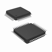
NUC100LC1BN
Description
IC MCU 32BIT 32KB FLASH 48LQFP
Manufacturer
Nuvoton Technology Corporation of America
Series
NuMicro™r
Specifications of NUC100LC1BN
Core Processor
ARM Cortex-M0
Core Size
32-Bit
Speed
50MHz
Connectivity
I²C, IrDA, SPI, UART/USART
Peripherals
Brown-out Detect/Reset, DMA, I²S, LVD, POR, PS2, PWM, WDT
Number Of I /o
35
Program Memory Size
32KB (32K x 8)
Program Memory Type
FLASH
Ram Size
4K x 8
Voltage - Supply (vcc/vdd)
2.5 V ~ 5.5 V
Data Converters
A/D 8x12b
Oscillator Type
Internal
Operating Temperature
-40°C ~ 85°C
Package / Case
48-LQFP
Lead Free Status / RoHS Status
Lead free / RoHS Compliant
Eeprom Size
-
Available stocks
Company
Part Number
Manufacturer
Quantity
Price
Company:

Part Number:
NUC100LC1BN
Manufacturer:
NuvoTon
Quantity:
1 600
Company:
Part Number:
NUC100LC1BN
Manufacturer:
Nuvoton Technology Corporation of America
Quantity:
10 000
Part Number:
NUC100LC1BN
Manufacturer:
NUVOTON
Quantity:
20 000


NuMicro™ NUC100 Series Technical Reference Manual
Figure 5-43 PWM Controller Output Duty Ratio........................................................................... 291
Figure 5-44 Paired-PWM Output with Dead Zone Generation Operation ................................... 291
Figure 5-45 Capture Operation Timing ........................................................................................ 292
Figure 5-46 PWM Group A PWM-Timer Interrupt Architecture Diagram..................................... 293
Figure 5-47 PWM Group B PWM-Timer Interrupt Architecture Diagram..................................... 293
Figure 5-48 RTC Block Diagram .................................................................................................. 323
Figure 5-49 SPI Block Diagram.................................................................................................... 342
Figure 5-50 SPI Master Mode Application Block Diagram........................................................... 343
Figure 5-51 SPI Slave Mode Application Block Diagram............................................................. 343
Figure 5-52 Variable Serial Clock Frequency .............................................................................. 345
Figure 5-53 32-Bit in one Transaction.......................................................................................... 345
Figure 5-54 Two Transactions in One Transfer (Burst Mode) ..................................................... 346
Figure 5-55 Byte Reorder............................................................................................................. 347
Figure 5-56 Timing Waveform for Byte Suspend......................................................................... 348
Figure 5-57 Two Bits Transfer Mode............................................................................................ 349
Figure 5-58 SPI Timing in Master Mode ...................................................................................... 350
Figure 5-59 SPI Timing in Master Mode (Alternate Phase of SPICLK) ....................................... 351
Figure 5-60 SPI Timing in Slave Mode ........................................................................................ 351
Figure 5-61 SPI Timing in Slave Mode (Alternate Phase of SPICLK) ......................................... 352
Figure 5-62 Timer Controller Block Diagram ............................................................................... 367
Figure 5-63 Clock Source of Timer Controller ............................................................................. 367
Figure 5-64 Timing of Interrupt and Reset Signal ........................................................................ 376
Figure 5-65 Watchdog Timer Clock Control................................................................................. 377
Figure 5-66 Watchdog Timer Block Diagram............................................................................... 377
Figure 5-67 UART Clock Control Diagram................................................................................... 384
Figure 5-68 UART Block Diagram................................................................................................ 384
Figure 5-69 Auto Flow Control Block Diagram............................................................................. 386
Figure 5-70 IrDA Block Diagram .................................................................................................. 387
Figure 5-71 IrDA TX/RX Timing Diagram .................................................................................... 388
Figure 5-72 Structure of LIN Frame ............................................................................................. 389
Figure 5-73 Structure of RS-485 Frame ...................................................................................... 391
Figure 5-74 CAN Bus Block Diagram........................................................................................... 420
Figure 5-75 Format of DATA FRAME .......................................................................................... 422
Figure 5-76 Standard Format in ARBITRATION FIELD .............................................................. 423
Figure 5-77 Extended Format in ARBITRATION FIELD.............................................................. 423
Figure 5-78 Format of CONTROL FIELD .................................................................................... 424
Figure 5-79 Format of CRC FIELD .............................................................................................. 425
Publication Release Date: Oct 22, 2010
- 9 -
Revision V1.06
Related parts for NUC100LC1BN
Image
Part Number
Description
Manufacturer
Datasheet
Request
R

Part Number:
Description:
Manufacturer:
Nuvoton Technology Corporation of America
Datasheet:
Part Number:
Description:
Manufacturer:
Nuvoton Technology Corporation of America
Datasheet:
Part Number:
Description:
Manufacturer:
Nuvoton Technology Corporation of America
Datasheet:
Part Number:
Description:
Manufacturer:
Nuvoton Technology Corporation of America
Datasheet:
Part Number:
Description:
Manufacturer:
Nuvoton Technology Corporation of America
Datasheet:
Part Number:
Description:
Manufacturer:
Nuvoton Technology Corporation of America
Datasheet:
Part Number:
Description:
Manufacturer:
Nuvoton Technology Corporation of America
Datasheet: