ATSAM3U-EK Atmel, ATSAM3U-EK Datasheet
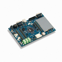
ATSAM3U-EK
Specifications of ATSAM3U-EK
Available stocks


Related parts for ATSAM3U-EK


ATSAM3U-EK Summary of contents
Page 1
Features • Core ® ® – ARM Cortex -M3 revision 2.0 running MHz – Memory Protection Unit (MPU) ® – Thumb -2 instruction set • Memories – From 64 to 256 Kbytes embedded Flash, 128-bit wide ...
Page 2
... SAM3U Description Atmel's SAM3U series is a member of a family of Flash microcontrollers based on the high per- formance 32-bit ARM Cortex-M3 RISC processor. It operates at a maximum speed of 96 MHz and features up to 256 Kbytes of Flash and Kbytes of SRAM. The peripheral set includes a High Speed USB Device port with embedded transceiver, a High Speed MCI for ...
Page 3
SAM3U Block Diagram Figure 2-1. 144-pin SAM3U4/2/1E Block Diagram MASTER SLAVE System Controller JTAG & Serial Wire TST PCK0 -PCK2 In-Circuit Emulator PLLA SysTick Counter UPLL Cortex-M3 Processor PMC Fmax 96 MHz OSC XIN 3-20 M XOUT MPU RC ...
Page 4
Figure 2-2. 100-pin SAM3U4/2/1C Block Diagram MASTER SLAVE JTAG & Serial Wire System Controller TST PCK0 -PCK2 In-Circuit Emulator PLLA SysTick Counter UPLL Cortex-M3 Processor PMC Fmax 96 MHz OSC XIN 3-20 M XOUT MPU RC Osc. I/D 12/8/4 M ...
Page 5
Signal Description Table 3-1 Table 3-1. Signal Description List Signal Name Function VDDIO Peripherals I/O Lines Power Supply VDDIN Voltage Regulator Input VDDOUT Voltage Regulator Output VDDUTMII USB UTMI+ Interface Power Supply GNDUTMII USB UTMI+ Interface Ground VDDBU Backup ...
Page 6
Table 3-1. Signal Description List (Continued) Signal Name Function ERASE Flash and NVM Configuration Bits Erase Command NRST Microcontroller Reset NRSTB Asynchronous Microcontroller Reset TST Test Select URXD UART Receive Data UTXD UART Transmit Data PA0 - PA31 Parallel IO ...
Page 7
Table 3-1. Signal Description List (Continued) Signal Name Function CK Multimedia Card Clock CDA Multimedia Card Slot A Command DA0 - DA7 Multimedia Card Slot A Data Universal Synchronous Asynchronous Receiver Transmitter - USARTx SCKx USARTx Serial Clock TXDx USARTx ...
Page 8
... TDO pin is set in input mode when the Cortex-M3 Core is not in debug mode. Thus an external pull-up (100 kΩ) must be added to avoid current consumption due to floating input. 3.1 Design Considerations In order to facilitate schematic capture when using a SAM3U design, Atmel provides a matics Checklist” Application note. Please visit SAM3U Series ...
Page 9
Package and Pinout The SAM3U4/2/1E is available in 144-lead LQFP and 144-ball LFBGA packages. The SAM3U4/2/1C is available in 100-lead LQFP and 100-ball LFBGA packages. 4.1 SAM3U4/2/1E Package and Pinout 4.1.1 144-ball LFBGA Package Outline The 144-Ball LFBGA package ...
Page 10
LQFP Pinout Table 4-1. 144-pin SAM3U4/2/1E Pinout 1 TDI 37 2 VDDOUT 38 3 VDDIN 39 4 TDO/TRACESWO 40 5 PB31 41 6 PB30 42 7 TMS/SWDIO 43 8 PB29 44 9 TCK/SWCLK 45 10 PB28 46 11 ...
Page 11
LFBGA Pinout Table 4-2. 144-ball SAM3U4/2/1E Pinout A1 VBG A2 VDDUTMI A3 PB9 A4 PB10 A5 PB19 A6 PC21 A7 PB26 A8 TCK/SWCLK A9 PB30 A10 TDO/TRACESWO A11 XIN32 A12 XOUT32 B1 VDDCORE B2 GNDUTMI B3 XOUT B4 ...
Page 12
SAM3U4/2/1C Package and Pinout 4.2.1 100-lead LQFP Package Outline Figure 4-3. 4.2.2 100-ball LFBGA Package Outline Figure 4-4. SAM3U Series 12 Orientation of the 100-lead LQFP Package 75 76 100 1 Orientation of the 100-ball LFBGA Package TOP VIEW ...
Page 13
LQFP Pinout Table 4-3. 100-pin SAM3U4/2/1C1 Pinout 1 VDDANA 2 ADVREF 3 GNDANA 4 AD12BVREF 5 PA22/PGMD14 6 PA30 7 PB3 8 PB4 9 VDDCORE 10 PA13/PGMD5 11 PA14/PGMD6 12 PA15/PGMD7 13 PA16/PGMD8 14 PA17/PGMD9 15 PB16 16 ...
Page 14
LFBGA Pinout Table 4-4. 100-ball SAM3U4/2/1C Pinout A1 VBG C6 A2 XIN C7 A3 XOUT C8 A4 PB17 C9 A5 PB21 C10 A6 PB23 D1 A7 TCK/SWCLK D2 A8 VDDIN D3 A9 VDDOUT D4 A10 XIN32 D5 B1 ...
Page 15
Power Considerations 5.1 Power Supplies The SAM3U product has several types of power supply pins: • VDDCORE pins: Power the core, the embedded memories and the peripherals; voltage ranges from 1.62V to 1.95V. • VDDIO pins: Power the Peripherals ...
Page 16
Figure 5-1. Note: SAM3U Series 16 Single Supply Main Supply (1.8V-3.6V) Restrictions With Main Supply < 2.0 V, USB and ADC are not usable. With Main Supply ≥ 2.4V and < 3V, USB is not usable. With Main Supply ≥ ...
Page 17
Figure 5-2. Note: 6430D–ATARM–25-Mar-11 Core Externally Supplied Main Supply (1.62V-3.6V) VDDCORE Supply (1.62V-1.95V) Restrictions With Main Supply < 2.0 V, USB and ADC are not usable. With Main Supply ≥ 2.4V and < 3V, USB is not usable. With Main ...
Page 18
Figure 5-3. Note: SAM3U Series 18 Backup Batteries Used Backup Batteries VDDBU Main Supply (1.62V-3.6V) Restrictions With Main Supply < 2.0 V, USB and ADC are not usable. With Main Supply ≥ 2.4V and < 3V, USB is not usable. ...
Page 19
Active Mode Active mode is the normal running mode with the core clock running from the fast RC oscillator, the main crystal oscillator or the PLLA. The power management controller can be used to adapt the frequency and to ...
Page 20
Entering Wait Mode: • Select the 4/8/12 MHz Fast RC Oscillator as Main Clock • Set the LPM bit in the PMC Fast Startup Mode Register (PMC_FSMR) • Execute the Wait-For-Event (WFE) instruction of the processor Note: 5.5.3 Sleep Mode ...
Page 21
Low Power Mode Summary Table The modes detailed above are the main low power modes. Each part can be set off sep- arately and wake up sources can be individually configured. of the configurations of the ...
Page 22
Wake-up Sources The wake-up events allow the device to exit backup mode. When a wake-up event is detected, the Supply Controller performs a sequence which automatically reenables the core power supply. Figure 5-4. Wake-up Source SMEN sm_int RTCEN rtc_alarm ...
Page 23
Fast Start-Up The SAM3U allows the processor to restart in a few microseconds while the processor is in wait mode. A fast start up can occur upon detection of a low level on one of the 19 wake-up inputs. ...
Page 24
Input/Output Lines The SAM3U has different kinds of input/output (I/O) lines, such as general purpose I/Os (GPIO) and system I/Os. GPIOs can have alternate functions thanks to multiplexing capabilities of the PIO controllers. The same GPIO line can be ...
Page 25
The JTAGSEL pin is used to select the JTAG boundary scan when asserted at a high level. It integrates a permanent pull-down resistor of about 15 kΩ to GNDBU, so that it can be left uncon- nected for normal operations. ...
Page 26
Even in all low power modes, asserting the pin will automatically start-up the chip and erase the Flash. 7. Processor and Architecture 7.1 ARM Cortex-M3 Processor • Version 2.0 • Thumb-2 (ISA) subset consisting of all base Thumb-2 instructions, 16-bit ...
Page 27
Matrix Slaves The Bus Matrix of the SAM3U manages 10 slaves. Each slave has its own arbiter, allowing a dif- ferent arbitration per slave. Table 7-2. Slave 0 Slave 1 Slave 2 Slave 3 Slave 4 Slave 5 Slave ...
Page 28
DMA Controller • Acting as one Matrix Master • Embeds 4 channels: – 3 channels with 8 bytes/FIFO for Channel Buffering – 1 channel with 32 bytes/FIFO for Channel Buffering • Linked List support with Status Write Back operation ...
Page 29
The Peripheral DMA Controller handles transfer requests from the channel according to the fol- lowing priorities (Low to High priorities): Table 7-5. Instance name UART USART3 USART2 USART1 USART0 UART USART3 USART2 USART1 USART0 ADC12B 7.8 Debug and Test Features ...
Page 30
Product Mapping Figure 8-1. SAM3U Memory Mapping Code 0x00000000 Boot Memory 0x00080000 Internal Flash 0 0x00100000 Internal Flash 1 0x00180000 Internal ROM 0x00200000 Reserved 0x1FFFFFFF Internal SRAM 0x20000000 SRAM0 1 MByte 0x20080000 bit band region SRAM1 0x20100000 NFC (SRAM) ...
Page 31
Memories The embedded and external memories are described below. 9.1 Embedded Memories 9.1.1 Internal SRAM The SAM3U4 (256 KBytes internal Flash version) embeds a total of 48 Kbytes high-speed SRAM (32 Kbytes SRAM0 and 16 Kbytes SRAM1). The SAM3U2 ...
Page 32
The Enhanced Embedded Flash Controller ensures the interface of the Flash block with the 32- bit internal bus. Its 128-bit wide memory interface increases performance. The user can choose between high performance or lower current consumption by selecting either 128-bit ...
Page 33
However safer to connect it directly to GND for the final application. 9.1.3.6 Calibration Bits NVM bits are used to calibrate the brownout detector and the voltage regulator. These bits are factory configured and cannot be changed ...
Page 34
Boot Strategies The system always boots at address 0x0. To ensure a maximum boot possibilities the memory layout can be changed via GPNVM. A general purpose NVM (GPNVM1) bit is used to boot either on the ROM (default) or ...
Page 35
Error Report, including error flag, correctable error flag and word address being – Supports 8- or 16-bit NAND Flash devices with 512-, 1024-, 2048- or 4096-byte 6430D–ATARM–25-Mar-11 detected erroneous pages SAM3U Series 35 ...
Page 36
System Controller The System Controller is a set of peripherals, which allow handling of key elements of the sys- tem, such as power, resets, clocks, time, interrupts, watchdog, etc... The System Controller User Interface also embeds the registers used ...
Page 37
Figure 10-1. System Controller Block Diagram VDDBU FWUP SHDN NRSTB Zero-Power Power-on Reset General Purpose Backup Registers SLCK RTC SLCK RTT osc32k_xtal_en XIN32 Xtal 32 kHz Oscillator XOUT32 Embedded 32 kHz RC osc32k_rc_en Oscillator Backup Power Supply vddcore_nreset NRST FSTT0 ...
Page 38
System Controller and Peripheral Mapping Please refer to All the peripherals are in the bit band region and are mapped in the bit band alias region. 10.2 Power-on-Reset, Brownout and Supply Monitor The SAM3U embeds three features to monitor, ...
Page 39
The Slow Clock generator is based kHz crystal oscillator and an embedded 32 kHz RC oscillator. The Slow Clock defaults to the RC oscillator, but the software can enable the crystal oscillator and select it as the ...
Page 40
Power Management Controller The Power Management Controller provides all the clock signals to the system. It provides: • the Processor Clock HCLK • the Free running processor clock FCLK • the Cortex SysTick external clock • the Master Clock ...
Page 41
Watchdog Timer • 16-bit key-protected once-only Programmable Counter • Windowed, prevents the processor dead-lock on the watchdog access 10.8 SysTick Timer • 24-bit down counter • Self-reload capability • Flexible system timer 10.9 Real-time Timer ...
Page 42
Chip Identification • Chip Identifier (CHIPID) registers permit recognition of the device and its revision. Table 10-1. Chip Name • JTAG ID: 0x0582A03F Table 10-2. Chip Name SAM3U4C (Rev A) SAM3U2C (Rev A) SAM3U1C (Rev A) SAM3U4E (Rev A) ...
Page 43
Synchronous output, provides Set and Clear of several I/O lines in a single write 6430D–ATARM–25-Mar-11 SAM3U Series 43 ...
Page 44
Peripherals 11.1 Peripheral Identifiers Table 11-1 the control of the peripheral interrupt with the Nested Vectored Interrupt Controller and for the control of the peripheral clock with the Power Management Controller. Note that some Peripherals are always clocked. Please ...
Page 45
Peripheral Signal Multiplexing on I/O Lines The SAM3U features 3 PIO controllers, PIOA, PIOB and PIOC that multiplex the I/O lines of the peripheral set. Each PIO Controller controls lines. Each line can be assigned to ...
Page 46
PIO Controller A Multiplexing Table 11-2. Multiplexing on PIO Controller A (PIOA) I/O Line Peripheral A PA0 TIOB0 PA1 TIOA0 PA2 TCLK0 PA3 MCCK PA4 MCCDA PA5 MCDA0 PA6 MCDA1 PA7 MCDA2 PA8 MCDA3 PA9 TWD0 PA10 TWCK0 PA11 ...
Page 47
PIO Controller B Multiplexing Table 11-3. Multiplexing on PIO Controller B (PIOB) I/O Line Peripheral A PB0 PWMH0 PB1 PWMH1 PB2 PWMH2 PWMH3 PB3 TCLK1 PB4 PB5 TIOA1 TIOB1 PB6 RTS0 PB7 PB8 CTS0 PB9 D0 D1 PB10 PB11 ...
Page 48
PIO Controller C Multiplexing Table 11-4. Multiplexing on PIO Controller C (PIOC) I/O Line Peripheral A PC0 A2 PC1 A3 PC2 A4 A5 PC3 A6 PC4 PC5 A7 A8 PC6 A9 PC7 PC8 A10 PC9 A11 A12 PC10 PC11 ...
Page 49
... Universal Asynchronous Receiver Transceiver (UART) • Two-pin UART – Implemented features are 100% compatible with the standard Atmel USART – Independent receiver and transmitter with a common programmable Baud Rate – Even, Odd, Mark or Space Parity Generation – Parity, Framing and Overrun Error Detection – ...
Page 50
Universal Synchronous Asynchronous Receiver Transmitter (USART) • Programmable Baud Rate Generator • 9-bit full-duplex synchronous or asynchronous serial communications – stop bits in Asynchronous Mode stop bits in Synchronous ...
Page 51
Pulse Generation – Delay Timing – Pulse Width Modulation – Up/Down Capabilities – Quadrature Decoder Logic • Each channel is user-configurable and contains: – Three external clock inputs – Five internal clock inputs – Two multi-purpose input/output signals • ...
Page 52
High Speed Multimedia Card Interface (HSMCI) • Compatibility with MultiMedia Card Specification Version 4.3 • Compatibility with SD Memory Card Specification Version 2.0 • Compatibility with SDIO Specification Version V2.0. • Compatibility with CE-ATA Specification 1.1 • Cards clock ...
Page 53
Selectable single ended or differential input voltage • Programmable gain for maximum full scale input range • External voltage reference for better accuracy on low voltage inputs • Individual enable and disable of each channel • Multiple trigger sources ...
Page 54
SAM3U Series 54 6430D–ATARM–25-Mar-11 ...
Page 55
... This material is for microcontroller software and hardware engineers, including those who have no experience of ARM products. Note: The information in this section is reproduced from source material provided to Atmel by ARM Ltd. in terms of Atmel’s license for the ARM Cortex is copyright ARM Ltd., 2008 - 2009. ...
Page 56
To facilitate the design of cost-sensitive devices, the Cortex-M3 processor implements tightly- coupled system components that reduce processor area while significantly improving interrupt handling and system ...
Page 57
Serial Wire Debug and Serial Wire Trace reduce the number of pins required for 13.2.4 Cortex-M3 core ...
Page 58
NVIC, or system control block • might have restricted access to memory or peripherals. Unprivileged software executes at the unprivileged level. 13.3.1.4 Privileged The software can use all the instructions and has access to ...
Page 59
Core registers The processor core registers are: Low registers High registers Stack Pointer Link Register Program Counter Table 13-2. Name R0-R12 MSP PSP LR PC PSR ASPR IPSR EPSR PRIMASK 6430D–ATARM–25-Mar- General-purpose ...
Page 60
Table 13-2. Name FAULTMASK BASEPRI CONTROL 1. 2. 13.3.3.1 General-purpose registers R0-R12 are 32-bit general-purpose registers for data operations. 13.3.3.2 Stack Pointer The Stack Pointer (SP) is register R13. In Thread mode, bit[1] of the CONTROL register indi- cates the ...
Page 61
Program Status Register The Program Status Register (PSR) combines: • Application Program Status Register (APSR) • Interrupt Program Status Register (IPSR) • Execution Program Status Register (EPSR). These registers are mutually exclusive bitfields in the 32-bit PSR. The bit ...
Page 62
The PSR bit assignments are Access these registers individually combination of any two or all three registers, using the register name as an argument to the MSR ...
Page 63
C Carry or borrow flag add operation did not result in a carry bit or subtract operation resulted in a borrow bit 1 = add operation resulted in a carry bit or subtract operation did not result ...
Page 64
Execution Program Status Register The EPSR contains the Thumb state bit, and the execution state bits for either the: • If-Then (IT) instruction • Interruptible-Continuable Instruction (ICI) field for an interrupted load multiple or store multiple instruction. See the ...
Page 65
Priority Mask Register The PRIMASK register prevents activation of all exceptions with configurable priority. See the register summary • PRIMASK effect 1 = prevents the activation of ...
Page 66
Base Priority Mask Register The BASEPRI register defines the minimum priority for exception processing. When BASEPRI is set to a nonzero value, it prevents the activation of all exceptions with same or lower priority level as the BASEPRI value. ...
Page 67
CONTROL register The CONTROL register controls the stack used and the privilege level for software execution when the processor is in Thread mode. See the register summary in its attributes. The bit assignments are ...
Page 68
Exceptions and interrupts The Cortex-M3 processor supports interrupts and system exceptions. The processor and the Nested Vectored Interrupt Controller (NVIC) prioritize and handle all exceptions. An exception changes the normal flow of software control. The processor uses handler mode ...
Page 69
CMSIS mapping of the Cortex-M3 NVIC registers” on page 167 • “NVIC programming hints” on page 6430D–ATARM–25-Mar-11 SAM3U Series 179. 69 ...
Page 70
Memory model This section describes the processor memory map, the behavior of memory accesses, and the bit-banding features. The processor has a fixed memory map that provides up to 4GB of addressable memory. The memory map is: The regions ...
Page 71
Normal The processor can re-order transactions for efficiency, or perform speculative reads. 13.4.1.2 Device The processor preserves transaction order relative to other transactions to Device or Strongly- ordered memory. 13.4.1.3 Strongly-ordered The processor preserves transaction order relative to all ...
Page 72
Means that accesses are observed in program order, that is always observed before A2. 13.4.3 Behavior of memory accesses The behavior of accesses to each region in the memory map is: Table 13-4. Address range 0x00000000- 0x1FFFFFFF ...
Page 73
Table 13-5. Address range 0x60000000- 0x7FFFFFFF 0x80000000- 0x9FFFFFFF 0xA0000000- 0xBFFFFFFF 0xC0000000- 0xDFFFFFFF 0xE0000000- 0xE00FFFFF 0xE0100000- 0xFFFFFFFF 1. 2. 13.4.4 Software ordering of memory accesses The order of instructions in the program flow does not always guarantee the order of the ...
Page 74
Use an ISB instruction to ensure the new MPU setting takes effect immediately after • Vector table. If the program changes an entry in the vector table, and then enables the corresponding exception, use a DMB instruction between the ...
Page 75
Table 13-7. Address range 0x40000000- 0x400FFFFF 0x42000000- 0x43FFFFFF A word access to the SRAM or peripheral bit-band alias regions map to a single bit in the SRAM or peripheral bit-band region. The following formula shows how the alias region maps ...
Page 76
Figure 13-2. Bit-band mapping 0x23FFFFFC 0x2200001C 7 7 13.4.5.1 Directly accessing an alias region Writing to a word in the alias region updates a single bit in the bit-band region. Bit[0] of the value written to a word in the ...
Page 77
Little-endian format In little-endian format, the processor stores the least significant byte of a word at the lowest- numbered byte, and the most significant byte at the highest-numbered byte. For example: Address A A+1 A+2 A+3 13.4.7 Synchronization primitives ...
Page 78
No write was performed. This indicates that the value returned the first step might be out of date. The software must retry the read-modify-write sequence, Software can use the synchronization primitives to implement a semaphores as follows: • Use ...
Page 79
Exception model This section describes the exception model. 13.5.1 Exception states Each exception is in one of the following states: 13.5.1.1 Inactive The exception is not active and not pending. 13.5.1.2 Pending The exception is waiting to be serviced ...
Page 80
Memory management fault A memory management fault is an exception that occurs because of a memory protection related fault. The MPU or the fixed memory protection constraints determines this fault, for both instruction and data memory transactions. This fault ...
Page 81
Interrupt (IRQ) A interrupt, or IRQ exception signalled by a peripheral, or generated by a software request. All interrupts are asynchronous to instruction execution. In the system, peripherals use interrupts to communicate with the processor. Table 13-9. ...
Page 82
Clear-enable Registers” on page For more information about hard faults, memory management faults, bus faults, and usage faults, see 13.5.3 Exception handlers The processor handles exceptions using: 13.5.3.1 Interrupt Service Routines (ISRs) Interrupts IRQ0 to IRQ29 are the ...
Page 83
Figure 13-3. Vector table On system reset, the vector table is fixed at address 0x00000000. Privileged software can write to the VTOR to relocate the vector table start address to a different memory location, in the range 0x00000080 to 0x3FFFFF80, ...
Page 84
Configurable priority values are in the range 0-15. This means that the Reset, Hard fault, and NMI exceptions, with fixed negative priority values, always have higher priority than any other exception. For example, assigning a higher priority value to IRQ[0] ...
Page 85
Tail-chaining This mechanism speeds up exception servicing. On completion of an exception handler, if there is a pending exception that meets the requirements for exception entry, the stack pop is skipped and control transfers to the new exception handler. ...
Page 86
If no higher priority exception occurs during exception entry, the processor starts executing the exception handler and automatically changes the status of the corresponding pending interrupt to active. If another higher priority exception occurs during exception entry, the processor starts ...
Page 87
BX instruction • attempting to execute an instruction from a memory region marked as Non-Executable • an MPU fault because of a privilege ...
Page 88
Usually, the exception priority, together with the values of the exception mask registers, deter- mines whether the processor enters the fault handler, and whether a fault handler can preempt another fault handler. as described in In some situations, a fault ...
Page 89
Power management The Cortex-M3 processor sleep modes reduce power consumption: • Backup Mode • Wait Mode • Sleep Mode The SLEEPDEEP bit of the SCR selects which sleep mode is used, see ter” on page Modes” in the PMC ...
Page 90
PRIMASK to zero. For more information about PRIMASK and FAULT- MASK see 13.7.2.2 Wakeup from WFE The processor wakes up if: • it detects an exception with sufficient priority to cause exception entry In addition, if ...
Page 91
Instruction set summary The processor implements a version of the Thumb instruction set. ported instructions. In Table • angle brackets, <>, enclose alternative forms of the operand • braces, {}, enclose optional operands • the Operands column is not ...
Page 92
Table 13-13. Cortex-M3 instructions (Continued) Mnemonic ISB IT LDM LDMDB, LDMEA LDMFD, LDMIA LDR LDRB, LDRBT LDRD LDREX LDREXB LDREXH LDRH, LDRHT LDRSB, LDRSBT LDRSH, LDRSHT LDRT LSL, LSLS LSR, LSRS MLA MLS MOV, MOVS MOVT MOVW, MOV MRS MSR ...
Page 93
Table 13-13. Cortex-M3 instructions (Continued) Mnemonic RBIT REV REV16 REVSH ROR, RORS RRX, RRXS RSB, RSBS SBC, SBCS SBFX SDIV SEV SMLAL SMULL SSAT STM STMDB, STMEA STMFD, STMIA STR STRB, STRBT STRD STREX STREXB STREXH STRH, STRHT STRT SUB, ...
Page 94
Table 13-13. Cortex-M3 instructions (Continued) Mnemonic TEQ TST UBFX UDIV UMLAL UMULL USAT UXTB UXTH WFE WFI 13.9 Intrinsic functions ANSI cannot directly access some Cortex-M3 instructions. This section describes intrinsic func- tions that can generate these instructions, provided by ...
Page 95
The CMSIS also provides a number of functions for accessing the special registers using MRS and MSR instructions: Table 13-15. CMSIS intrinsic functions to access the special registers Special register PRIMASK FAULTMASK BASEPRI CONTROL MSP PSP 13.10 About the instruction ...
Page 96
Bit[0] of any address you write to the PC with a BX, BLX, LDM, LDR, or POP instruction must be 1 for correct execution, because this bit indicates the required instruction set, and the Cortex-M3 processor only supports Thumb instructions. ...
Page 97
LSR #n ROR #n RRX - If you omit the shift, or specify LSL #0, the instruction uses the value in Rm. If you specify a shift, the shift is applied to the value in Rm, and the resulting 32-bit ...
Page 98
LSR Logical shift right by n bits moves the left-hand 32-n bits of the register Rm, to the right by n places, into the right-hand 32-n bits of the result. And it sets the left-hand n bits of the ...
Page 99
ROR Rotate right by n bits moves the left-hand 32-n bits of the register Rm, to the right by n places, into the right-hand 32-n bits of the result. And it moves the right-hand n bits of the register ...
Page 100
All other load and store instructions generate a usage fault exception if they perform an unaligned access, and therefore their accesses must be address aligned. For more information about usage faults see Unaligned accesses are usually slower than aligned accesses. ...
Page 101
Use the CBZ and CBNZ instructions to compare the value of a register against zero and branch on the result. This section describes: • “The condition flags” • “Condition code 13.10.7.1 The condition flags The APSR contains the following condition ...
Page 102
Table 13-16. Condition code suffixes (Continued) Suffix 13.10.7.3 Absolute value The example below shows the use of a conditional instruction to find the absolute value of a number ...
Page 103
Memory access instructions Table 13-17 Table 13-17. Memory access instructions Mnemonic ADR CLREX LDM{mode} LDR{type} LDR{type} LDR{type}T LDR LDREX{type} POP PUSH STM{mode} STR{type} STR{type} STR{type}T STREX{type} 6430D–ATARM–25-Mar-11 shows the memory access instructions: Brief description Load PC-relative address Clear Exclusive ...
Page 104
ADR Load PC-relative address. 13.11.1.1 Syntax ADR{cond} Rd, label where: cond Rd label 13.11.1.2 Operation ADR determines the address by adding an immediate value to the PC, and writes the result to the destination register. ADR produces position-independent code, ...
Page 105
LDR and STR, immediate offset Load and Store with immediate offset, pre-indexed immediate offset, or post-indexed immediate offset. 13.11.2.1 Syntax op{type}{cond} Rt, [Rn {, #offset}] op{type}{cond} Rt, [Rn, #offset]! op{type}{cond} Rt, [Rn], #offset opD{cond} Rt, Rt2, [Rn {, #offset}] ...
Page 106
Post-indexed addressing The address obtained from the register Rn is used as the address for the memory access. The offset value is added to or subtracted from the address, and written back into the register Rn. The ...
Page 107
Examples LDR R8, [R10] LDRNE R2, [R5, #960]! STR R2, [R9,#const-struc] STRH R3, [R4], #4 LDRD R8, R9, [R3, #0x20] STRD R0, R1, [R8], #-16 6430D–ATARM–25-Mar-11 ; Loads R8 from the address in R10. ; Loads (conditionally) R2 from ...
Page 108
LDR and STR, register offset Load and Store with register offset. 13.11.3.1 Syntax op{type}{cond} Rt, [Rn LSL #n}] where: op LDR STR type cond LSL #n 13.11.3.2 Operation LDR ...
Page 109
Condition flags These instructions do not change the flags. 13.11.3.5 Examples STR R0, [R5, R1] LDRSB R0, [R5, R1, LSL #1] ; Read byte value from an address equal to STR R0, [R1, R2, LSL #2] ; Stores R0 ...
Page 110
LDR and STR, unprivileged Load and Store with unprivileged access. 13.11.4.1 Syntax op{type}T{cond} Rt, [Rn {, #offset}] where: op LDR STR type is one of cond Rt Rn offset 13.11.4.2 Operation These load and ...
Page 111
LDR, PC-relative Load register from memory. 13.11.5.1 Syntax LDR{type}{cond} Rt, label LDRD{cond} Rt, Rt2, label where: type cond Rt Rt2 label 13.11.5.2 Operation LDR loads a register with a value from a PC-relative memory ...
Page 112
IT block. 13.11.5.4 Condition flags These ...
Page 113
LDM and STM Load and Store Multiple registers. 13.11.6.1 Syntax op{addr_mode}{cond} Rn{!}, reglist where: op LDM STM addr_mode IA DB cond present the final address, that is loaded from or stored to, is written ...
Page 114
The accesses happen in order of decreasing register numbers, with the highest numbered regis- ter using the highest memory address and the lowest number register using the lowest memory address. If the writeback suffix is specified, the value of Rn ...
Page 115
PUSH and POP Push registers onto, and pop registers off a full-descending stack. 13.11.7.1 Syntax PUSH{cond} reglist POP{cond} reglist where: cond reglist It must be comma separated if it contains more than one register or register range. PUSH and ...
Page 116
LDREX and STREX Load and Store Register Exclusive. 13.11.8.1 Syntax LDREX{cond} Rt, [Rn {, #offset}] STREX{cond} Rd, Rt, [Rn {, #offset}] LDREXB{cond} Rt, [Rn] STREXB{cond} Rd, Rt, [Rn] LDREXH{cond} Rt, [Rn] STREXH{cond} Rd, Rt, [Rn] where: cond Rd Rt ...
Page 117
Condition flags These instructions do not change the flags. 13.11.8.5 Examples MOV R1, #0x1 try LDREX R0, [LockAddr] CMP R0, #0 ITT EQ STREXEQ R0, R1, [LockAddr] CMPEQ R0, #0 BNE try .... 6430D–ATARM–25-Mar-11 ; Initialize the ‘lock taken’ ...
Page 118
CLREX Clear Exclusive. 13.11.9.1 Syntax CLREX{cond} where: cond 13.11.9.2 Operation Use CLREX to make the next STREX, STREXB, or STREXH instruction write 1 to its destination register and fail to perform the store useful in exception handler ...
Page 119
General data processing instructions Table 13-20 Table 13-20. Data processing instructions Mnemonic ADC ADD ADDW AND ASR BIC CLZ CMN CMP EOR LSL LSR MOV MOVT MOVW MVN ORN ORR RBIT REV REV16 REVSH ROR 6430D–ATARM–25-Mar-11 shows the data ...
Page 120
Table 13-20. Data processing instructions (Continued) Mnemonic RRX RSB SBC SUB SUBW TEQ TST SAM3U Series 120 Brief description Rotate Right with Extend Reverse Subtract Subtract with Carry Subtract Subtract Test Equivalence Test See “ASR, LSL, LSR, ROR, and RRX” ...
Page 121
ADD, ADC, SUB, SBC, and RSB Add, Add with carry, Subtract, Subtract with carry, and Reverse Subtract. 13.12.1.1 Syntax op{S}{cond} {Rd,} Rn, Operand2 op{cond} {Rd,} Rn, #imm12 where: op ADD ADC SUB SBC RSB S result of the operation, ...
Page 122
Rd can be SP only in ADD and SUB, and only with the additional restrictions: – Rn must also be SP – any shift in Operand2 must be limited to a maximum of 3 bits using LSL • Rn ...
Page 123
Multiword arithmetic examples 13.12.1.7 64-bit addition The example below shows two instructions that add a 64-bit integer contained in R2 and R3 to another 64-bit integer con- tained in R0 and R1, and place the result in R4 and ...
Page 124
AND, ORR, EOR, BIC, and ORN Logical AND, OR, Exclusive OR, Bit Clear, and OR NOT. 13.12.2.1 Syntax op{S}{cond} {Rd,} Rn, Operand2 where: op AND ORR EOR BIC ORN S result of the operation, see cond Rd Rn Operand2 ...
Page 125
Examples AND R9, R2, #0xFF00 ORREQ R2, R0, R5 ANDS R9, R8, #0x19 EORS R7, R11, #0x18181818 BIC R0, R1, #0xab ORN R7, R11, R14, ROR #4 ORNS R7, R11, R14, ASR #32 6430D–ATARM–25-Mar-11 SAM3U Series 125 ...
Page 126
ASR, LSL, LSR, ROR, and RRX Arithmetic Shift Right, Logical Shift Left, Logical Shift Right, Rotate Right, and Rotate Right with Extend. 13.12.3.1 Syntax op{S}{cond} Rd, Rm, Rs op{S}{cond} Rd, Rm, #n RRX{S}{cond} Rd, Rm where: op ASR LSL ...
Page 127
C flag is updated to the last bit shifted out, except when the shift length is 0, see Operations” on page 13.12.3.5 Examples ASR R7, R8 Arithmetic shift right by 9 bits LSLS R1, R2, #3 ...
Page 128
CLZ Count Leading Zeros. 13.12.4.1 Syntax CLZ{cond} Rd, Rm where: cond Rd Rm 13.12.4.2 Operation The CLZ instruction counts the number of leading zeros in the value in Rm and returns the result in Rd. The result value is ...
Page 129
CMP and CMN Compare and Compare Negative. 13.12.5.1 Syntax CMP{cond} Rn, Operand2 CMN{cond} Rn, Operand2 where: cond Rn Operand2 details of the options. 13.12.5.2 Operation These instructions compare the value in a register with Operand2. They update the condition ...
Page 130
MOV and MVN Move and Move NOT. 13.12.6.1 Syntax MOV{S}{cond} Rd, Operand2 MOV{cond} Rd, #imm16 MVN{S}{cond} Rd, Operand2 where: S result of the operation, see cond Rd Operand2 details of the options. imm16 13.12.6.2 Operation The MOV instruction copies ...
Page 131
PC is ignored • a branch occurs to the address created by forcing bit[0] of that value to 0. Though it is possible to use MOV as a branch instruction, ARM strongly ...
Page 132
MOVT Move Top. 13.12.7.1 Syntax MOVT{cond} Rd, #imm16 where: cond Rd imm16 13.12.7.2 Operation MOVT writes a 16-bit immediate value, imm16, to the top halfword, Rd[31:16], of its destination register. The write does not affect Rd[15:0]. The MOV, MOVT ...
Page 133
REV, REV16, REVSH, and RBIT Reverse bytes and Reverse bits. 13.12.8.1 Syntax op{cond} Rd, Rn where: op REV REV16 Reverse byte order in each halfword independently. REVSH Reverse byte order in the bottom halfword, and sign extend to 32 ...
Page 134
TST and TEQ Test bits and Test Equivalence. 13.12.9.1 Syntax TST{cond} Rn, Operand2 TEQ{cond} Rn, Operand2 where: cond Rn Operand2 details of the options. 13.12.9.2 Operation These instructions test the value in a register against Operand2. They update the ...
Page 135
Multiply and divide instructions Table 13-21 Table 13-21. Multiply and divide instructions Mnemonic MLA MLS MUL SDIV SMLAL SMULL UDIV UMLAL UMULL 6430D–ATARM–25-Mar-11 shows the multiply and divide instructions: Brief description Multiply with Accumulate, 32-bit result Multiply and Subtract, ...
Page 136
MUL, MLA, and MLS Multiply, Multiply with Accumulate, and Multiply with Subtract, using 32-bit operands, and pro- ducing a 32-bit result. 13.13.1.1 Syntax MUL{S}{cond} {Rd,} Rn Multiply MLA{cond} Rd, Rn, Rm, Ra MLS{cond} Rd, Rn, Rm, Ra ...
Page 137
UMULL, UMLAL, SMULL, and SMLAL Signed and Unsigned Long Multiply, with optional Accumulate, using 32-bit operands and pro- ducing a 64-bit result. 13.13.2.1 Syntax op{cond} RdLo, RdHi, Rn, Rm where: op UMULL Unsigned Long Multiply. UMLAL Unsigned Long Multiply, ...
Page 138
SDIV and UDIV Signed Divide and Unsigned Divide. 13.13.3.1 Syntax SDIV{cond} {Rd,} Rn, Rm UDIV{cond} {Rd,} Rn, Rm where: cond 13.13.3.2 Operation SDIV performs a signed integer division of the value the value ...
Page 139
Saturating instructions This section describes the saturating instructions, SSAT and USAT. 13.14.1 SSAT and USAT Signed Saturate and Unsigned Saturate to any bit position, with optional shift before saturating. 13.14.1.1 Syntax op{cond} Rd, # shift #s} where: ...
Page 140
Restrictions Do not use SP and do not use PC 13.14.1.4 Condition flags These instructions do not affect the condition code flags. If saturation occurs, these instructions set the Q flag to 1. 13.14.1.5 Examples SSAT R7, #16, R7, ...
Page 141
Bitfield instructions Table 13-22 Table 13-22. Packing and unpacking instructions Mnemonic BFC BFI SBFX SXTB SXTH UBFX UXTB UXTH 6430D–ATARM–25-Mar-11 shows the instructions that operate on adjacent sets of bits in registers or bitfields: Brief description Bit Field Clear ...
Page 142
BFC and BFI Bit Field Clear and Bit Field Insert. 13.15.1.1 Syntax BFC{cond} Rd, #lsb, #width BFI{cond} Rd, Rn, #lsb, #width where: cond Rd Rn lsb width 13.15.1.2 Operation BFC clears a bitfield in a register. It clears width ...
Page 143
SBFX and UBFX Signed Bit Field Extract and Unsigned Bit Field Extract. 13.15.2.1 Syntax SBFX{cond} Rd, Rn, #lsb, #width UBFX{cond} Rd, Rn, #lsb, #width where: cond Rd Rn lsb width 13.15.2.2 Operation SBFX extracts a bitfield from one register, ...
Page 144
SXT and UXT Sign extend and Zero extend. 13.15.3.1 Syntax SXTextend{cond} {Rd ROR #n} UXTextend{cond} {Rd ROR #n} where: extend B H cond Rd Rm ROR #n ROR #8 Value from Rm is rotated right ...
Page 145
Branch and control instructions Table 13-23 Table 13-23. Branch and control instructions Mnemonic B BL BLX BX CBNZ CBZ IT TBB TBH 6430D–ATARM–25-Mar-11 shows the branch and control instructions: Brief description Branch Branch with Link Branch indirect with Link ...
Page 146
B, BL, BX, and BLX Branch instructions. 13.16.1.1 Syntax B{cond} label BL{cond} label BX{cond} Rm BLX{cond} Rm where BLX cond label but the address to branch to is created by changing bit[0] to ...
Page 147
PC in the BLX instruction • for BX and BLX, bit[ must be 1 for correct execution but a branch occurs to the target address created by changing bit[ • when any ...
Page 148
CBZ and CBNZ Compare and Branch on Zero, Compare and Branch on Non-Zero. 13.16.2.1 Syntax CBZ Rn, label CBNZ Rn, label where: Rn label 13.16.2.2 Operation Use the CBZ or CBNZ instructions to avoid changing the condition code flags ...
Page 149
IT If-Then condition instruction. 13.16.3.1 Syntax IT{x{y{z}}} cond where cond The condition switch for the second, third and fourth instruction in the IT block can be either possible to use AL (the ...
Page 150
PC must either be outside an IT block or must be the last instruction inside the IT block. These are: – ADD PC, PC, Rm – MOV PC, Rm – B, ...
Page 151
TBB and TBH Table Branch Byte and Table Branch Halfword. 13.16.4.1 Syntax TBB [Rn, Rm] TBH [Rn, Rm, LSL #1] where: Rn then the address of the table is the address of the byte immediately following the TBB or ...
Page 152
Examples ADR.W R0, BranchTable_Byte TBB [R0, R1] Case1 ; an instruction sequence follows Case2 ; an instruction sequence follows Case3 ; an instruction sequence follows BranchTable_Byte DCB 0 DCB ((Case2-Case1)/2) DCB ((Case3-Case1)/2) TBH [PC, R1, LSL #1] BranchTable_H DCI ...
Page 153
Miscellaneous instructions Table 13-25 Table 13-25. Miscellaneous instructions Mnemonic BKPT CPSID CPSIE DMB DSB ISB MRS MSR NOP SEV SVC WFE WFI 6430D–ATARM–25-Mar-11 shows the remaining Cortex-M3 instructions: Brief description Breakpoint Change Processor State, Disable Interrupts Change Processor State, ...
Page 154
BKPT Breakpoint. 13.17.1.1 Syntax BKPT #imm where: imm 13.17.1.2 Operation The BKPT instruction causes the processor to enter Debug state. Debug tools can use this to investigate system state when the instruction at a particular address is reached. imm ...
Page 155
CPS Change Processor State. 13.17.2.1 Syntax CPSeffect iflags where: effect IE ID iflags i f 13.17.2.2 Operation CPS changes the PRIMASK and FAULTMASK special register values. See registers” on page 64 13.17.2.3 Restrictions The restrictions are: • use CPS ...
Page 156
DMB Data Memory Barrier. 13.17.3.1 Syntax DMB{cond} where: cond 13.17.3.2 Operation DMB acts as a data memory barrier. It ensures that all explicit memory accesses that appear, in program order, before the DMB instruction are completed before any explicit ...
Page 157
DSB Data Synchronization Barrier. 13.17.4.1 Syntax DSB{cond} where: cond 13.17.4.2 Operation DSB acts as a special data synchronization memory barrier. Instructions that come after the DSB, in program order, do not execute until the DSB instruction completes. The DSB ...
Page 158
ISB Instruction Synchronization Barrier. 13.17.5.1 Syntax ISB{cond} where: cond 13.17.5.2 Operation ISB acts as an instruction synchronization barrier. It flushes the pipeline of the processor, so that all instructions following the ISB are fetched from memory again, after the ...
Page 159
MRS Move the contents of a special register to a general-purpose register. 13.17.6.1 Syntax MRS{cond} Rd, spec_reg where: cond Rd spec_reg PRIMASK, BASEPRI, BASEPRI_MAX, FAULTMASK, or CONTROL. 13.17.6.2 Operation Use MRS in combination with MSR as part of a ...
Page 160
MSR Move the contents of a general-purpose register into the specified special register. 13.17.7.1 Syntax MSR{cond} spec_reg, Rn where: cond Rn spec_reg PRIMASK, BASEPRI, BASEPRI_MAX, FAULTMASK, or CONTROL. 13.17.7.2 Operation The register access operation in MSR depends on the ...
Page 161
NOP No Operation. 13.17.8.1 Syntax NOP{cond} where: cond 13.17.8.2 Operation NOP does nothing. NOP is not necessarily a time-consuming NOP. The processor might remove it from the pipeline before it reaches the execution stage. Use NOP for padding, for ...
Page 162
SEV Send Event. 13.17.9.1 Syntax SEV{cond} where: cond 13.17.9.2 Operation SEV is a hint instruction that causes an event to be signaled to all processors within a multipro- cessor system. It also sets the local event register to 1, ...
Page 163
SVC Supervisor Call. 13.17.10.1 Syntax SVC{cond} #imm where: cond imm 13.17.10.2 Operation The SVC instruction causes the SVC exception. imm is ignored by the processor. If required, it can be retrieved by the exception handler to determine what service ...
Page 164
WFE Wait For Event. 13.17.11.1 Syntax WFE{cond} where: cond 13.17.11.2 Operation WFE is a hint instruction. If the event register is 0, WFE suspends execution until one of the following events occurs: • an exception, unless masked by the ...
Page 165
WFI Wait for Interrupt. 13.17.12.1 Syntax WFI{cond} where: cond 13.17.12.2 Operation WFI is a hint instruction that suspends execution until one of the following events occurs: • an exception • a Debug Entry request, regardless of whether Debug is ...
Page 166
About the Cortex-M3 The address map of the Private peripheral bus (PPB) is: Table 13-26. Core peripheral register regions Address 0xE000E008- 0xE000E00F 0xE000E010- 0xE000E01F 0xE000E100- 0xE000E4EF 0xE000ED00- 0xE000ED3F 0xE000ED90- 0xE000EDB8 0xE000EF00- 0xE000EF03 In register descriptions: • the register type ...
Page 167
Nested Vectored Interrupt Controller This section describes the Nested Vectored Interrupt Controller (NVIC) and the registers it uses. The NVIC supports: • interrupts. • A programmable priority level of 0-15 for each interrupt. A higher level ...
Page 168
Interrupt Priority Registers map to an array of 4-bit integers, so that the array IP[0] to IP[29] corresponds to the registers IPR0-IPR7, and the array entry IP[n] holds the interrupt priority for interrupt n. ...
Page 169
Interrupt Set-enable Registers The ISER0 register enables interrupts, and show which interrupts are enabled. See: • the register summary in • Table 13-28 on page 168 The bit assignments are • ...
Page 170
Interrupt Clear-enable Registers The ICER0 register disables interrupts, and shows which interrupts are enabled. See: • the register summary in • Table 13-28 on page 168 The bit assignments are • ...
Page 171
Interrupt Set-pending Registers The ISPR0 register forces interrupts into the pending state, and shows which interrupts are pending. See: • the register summary in • Table 13-28 on page 168 The bit assignments are ...
Page 172
Interrupt Clear-pending Registers The ICPR0 register removes the pending state from interrupts, and show which interrupts are pending. See: • the register summary in • Table 13-28 on page 168 The bit assignments are ...
Page 173
Interrupt Active Bit Registers The IABR0 register indicates which interrupts are active. See: • the register summary in • Table 13-28 on page 168 The bit assignments are • ACTIVE Interrupt ...
Page 174
Interrupt Priority Registers The IPR0-IPR7 registers provide a 4-bit priority field for each interrupt (See the “Peripheral Iden- tifiers” section of the datasheet for more details). These registers are byte-accessible. See the register summary in fields, that map up ...
Page 175
IPR2 13.19.7.5 IPR1 13.19.7.6 IPR0 • Priority, byte offset 3 • Priority, byte offset 2 ...
Page 176
Find the IPR number and byte offset for interrupt N as follows: • the corresponding IPR number given DIV 4 • the byte offset of the required Priority field in this register is N ...
Page 177
Software Trigger Interrupt Register Write to the STIR to generate a Software Generated Interrupt (SGI). See the register summary in Table 13-27 on page 167 When the USERSETMPEND bit in the SCR is set to 1, unprivileged software can ...
Page 178
Level-sensitive interrupts The processor supports level-sensitive interrupts. A level-sensitive interrupt is held asserted until the peripheral deasserts the interrupt signal. Typ- ically this happens because the ISR accesses the peripheral, causing it to clear the interrupt request. When the ...
Page 179
NVIC design hints and tips Ensure software uses correctly aligned register accesses. The processor does not support unaligned accesses to NVIC registers. See the individual register descriptions for the supported access sizes. A interrupt can enter pending state even ...
Page 180
System control block The System control block (SCB) provides system implementation information, and system con- trol. This includes configuration, control, and reporting of the system exceptions. The system control block registers are: Table 13-30. Summary of the system control ...
Page 181
Auxiliary Control Register The ACTLR provides disable bits for the following processor functions: • IT folding • write buffer use for accesses to the default memory map • interruption of multi-cycle instructions. See the register summary in ments are: ...
Page 182
CPUID Base Register The CPUID register contains the processor part number, version, and implementation informa- tion. See the register summary in are Variant PartNo • Implementer Implementer code: 0x41 = ARM ...
Page 183
Interrupt Control and State Register The ICSR: • provides: – set-pending and clear-pending bits for the PendSV and SysTick exceptions • indicates: – the exception number of the exception being processed – whether there are preempted active exceptions – ...
Page 184
PENDSTSET RW SysTick exception set-pending bit. Write effect 1 = changes SysTick exception state to pending. Read SysTick exception is not pending 1 = SysTick exception is pending. • PENDSTCLR WO SysTick exception clear-pending ...
Page 185
RETTOBASE RO Indicates whether there are preempted active exceptions there are preempted active exceptions to execute 1 = there are no active exceptions, or the currently-executing exception is the only active exception. • VECTACTIVE RO Contains the ...
Page 186
Vector Table Offset Register The VTOR indicates the offset of the vector table base address from memory address 0x00000000. See the register summary in The bit assignments are Reserved TBLOFF • ...
Page 187
Application Interrupt and Reset Control Register The AIRCR provides priority grouping control for the exception model, endian status for data accesses, and reset control of the system. See the register summary in 180 and To write to this register, ...
Page 188
VECTCLRACTIVE WO Reserved for Debug use. This bit reads as 0. When writing to the register you must write 0 to this bit, otherwise behavior is Unpredictable. • VECTRESET WO Reserved for Debug use. This bit reads as 0. ...
Page 189
System Control Register The SCR controls features of entry to and exit from low power state. See the register summary in Table 13-30 on page 180 Reserved • SEVONPEND Send Event ...
Page 190
Configuration and Control Register The CCR controls entry to Thread mode and enables: • the handlers for hard fault and faults escalated by FAULTMASK to ignore bus faults • trapping of divide by zero and unaligned accesses • access ...
Page 191
If this bit is set unaligned access generates a usage fault. Unaligned LDM, STM, LDRD, and STRD instructions always fault irrespective of whether UNALIGN_TRP is set to 1. • ...
Page 192
System Handler Priority Registers The SHPR1-SHPR3 registers set the priority level the exception handlers that have configurable priority. SHPR1-SHPR3 are byte accessible. See the register summary in their attributes. The system fault handlers and the ...
Page 193
System Handler Priority Register 1 The bit assignments are • PRI_7 Reserved • PRI_6 Priority of system handler 6, usage fault • PRI_5 Priority of system handler 5, bus fault • ...
Page 194
System Handler Priority Register 2 The bit assignments are • PRI_11 Priority of system handler 11, SVCall 13.20.9.3 System Handler Priority Register 3 The bit assignments are ...
Page 195
System Handler Control and State Register The SHCSR enables the system handlers, and indicates: • the pending status of the bus fault, memory management fault, and SVC exceptions • the active status of the system handlers. See the register ...
Page 196
MONITORACT Debug monitor active bit, reads Debug monitor is active • SVCALLACT SVC call active bit, reads SVC call is active • USGFAULTACT Usage fault exception active bit, reads exception ...
Page 197
Configurable Fault Status Register The CFSR indicates the cause of a memory management fault, bus fault, or usage fault. See the register summary The following subsections describe the subregisters that ...
Page 198
Memory Management Fault Status Register The flags in the MMFSR indicate the cause of memory access faults. The bit assignments are MMARVALID Reserved • MMARVALID Memory Management Fault Address Register (MMAR) valid flag value in ...
Page 199
Bus Fault Status Register The flags in the BFSR indicate the cause of a bus access fault. The bit assignments are BFRVALID Reserved • BFARVALID Bus Fault Address Register (BFAR) valid flag value in BFAR ...
Page 200
PRECISERR Precise data bus error precise data bus error data bus error has occurred, and the PC value stacked for the exception return points to the instruction that caused the fault. When the ...