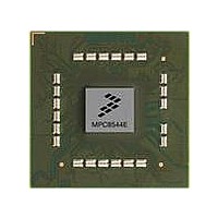
MPC8544DS Freescale Semiconductor, MPC8544DS Datasheet - Page 275

MPC8544DS
Manufacturer Part Number
MPC8544DS
Description
BOARD DEVELOPMENT SYSTEM 8544
Manufacturer
Freescale Semiconductor
Series
PowerQUICC III™r
Type
MPUr
Datasheets
1.MPC8544VTALF.pdf
(117 pages)
2.MPC8544VTALF.pdf
(2 pages)
3.MPC8544VTALF.pdf
(1340 pages)
4.MPC8544DS.pdf
(2 pages)
Specifications of MPC8544DS
Contents
Board
Processor To Be Evaluated
MPC8544E
Data Bus Width
32 bit
Interface Type
Ethernet, I2C
Operating Supply Voltage
- 0.3 V to + 1.1 V
Leaded Process Compatible
Yes
Peak Reflow Compatible (260 C)
Yes
Rohs Compliant
Yes
For Use With/related Products
MPC8544
For Use With
PPC8544EVTANG - EVAL MPC8544 783FCPBGA
Lead Free Status / RoHS Status
Lead free / RoHS Compliant
- MPC8544VTALF PDF datasheet
- MPC8544VTALF PDF datasheet #2
- MPC8544VTALF PDF datasheet #3
- MPC8544DS PDF datasheet #4
- Current page: 275 of 1340
- Download datasheet (12Mb)
7.2.1
Figure 7-3
Physical address bits 21–30 identify the bank and set of the tag and data. Physical address bits 0–20 are
compared against the tags of all eight ways. A match of a valid tag selects a 32-byte block of data (or way)
within the set. Physical address bits 31–35 identify the byte or bytes of data within the block.
7.2.2
When all or part of the array is dedicated to memory mapped SRAM, individual ways of each set are
reserved for that purpose. SRAM accesses use physical address bits 18–20 in conjunction with the SRAM
mode to select a way of the indexed set.
Freescale Semiconductor
Tag Lookup
Way Select
Data Read/Write
shows how physical address bits are used to access the L2 cache.
Accessing the On-Chip Array as an L2 Cache
Accessing the On-Chip Array as an SRAM
MPC8544E PowerQUICC III Integrated Host Processor Family Reference Manual, Rev. 1
Figure 7-3. Physical Address Usage for L2 Cache Accesses
Bank select
21
0
21
Bank select
22 23
22 23
ADDR
ADDR
Set index
Set index
(8 bits)
(8 bits)
ADDR
Tags (21 bits)
30
30
Tag Compare
Way select
(3 bits)
Way
31
20
Byte select
(5 bits)
ADDR
35
8 Tags per Set
L2 Look-Aside Cache/SRAM
7-5
Related parts for MPC8544DS
Image
Part Number
Description
Manufacturer
Datasheet
Request
R
Part Number:
Description:
Manufacturer:
Freescale Semiconductor, Inc
Datasheet:
Part Number:
Description:
Manufacturer:
Freescale Semiconductor, Inc
Datasheet:
Part Number:
Description:
Manufacturer:
Freescale Semiconductor, Inc
Datasheet:
Part Number:
Description:
Manufacturer:
Freescale Semiconductor, Inc
Datasheet:
Part Number:
Description:
Manufacturer:
Freescale Semiconductor, Inc
Datasheet:
Part Number:
Description:
Manufacturer:
Freescale Semiconductor, Inc
Datasheet:
Part Number:
Description:
Manufacturer:
Freescale Semiconductor, Inc
Datasheet:
Part Number:
Description:
Manufacturer:
Freescale Semiconductor, Inc
Datasheet:
Part Number:
Description:
Manufacturer:
Freescale Semiconductor, Inc
Datasheet:
Part Number:
Description:
Manufacturer:
Freescale Semiconductor, Inc
Datasheet:
Part Number:
Description:
Manufacturer:
Freescale Semiconductor, Inc
Datasheet:
Part Number:
Description:
Manufacturer:
Freescale Semiconductor, Inc
Datasheet:
Part Number:
Description:
Manufacturer:
Freescale Semiconductor, Inc
Datasheet:
Part Number:
Description:
Manufacturer:
Freescale Semiconductor, Inc
Datasheet:
Part Number:
Description:
Manufacturer:
Freescale Semiconductor, Inc
Datasheet:


