MPC8544DS Freescale Semiconductor, MPC8544DS Datasheet - Page 472
MPC8544DS
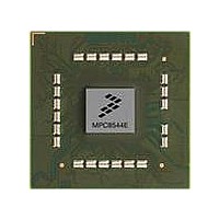
Manufacturer Part Number
MPC8544DS
Description
BOARD DEVELOPMENT SYSTEM 8544
Manufacturer
Freescale Semiconductor
Series
PowerQUICC III™r
Type
MPUr
Datasheets
1.MPC8544VTALF.pdf
(117 pages)
2.MPC8544VTALF.pdf
(2 pages)
3.MPC8544VTALF.pdf
(1340 pages)
4.MPC8544DS.pdf
(2 pages)
Specifications of MPC8544DS
Contents
Board
Processor To Be Evaluated
MPC8544E
Data Bus Width
32 bit
Interface Type
Ethernet, I2C
Operating Supply Voltage
- 0.3 V to + 1.1 V
Leaded Process Compatible
Yes
Peak Reflow Compatible (260 C)
Yes
Rohs Compliant
Yes
For Use With/related Products
MPC8544
For Use With
PPC8544EVTANG - EVAL MPC8544 783FCPBGA
Lead Free Status / RoHS Status
Lead free / RoHS Compliant


I
The sequence repeats with successive targets until the CONT bit in the data structure is cleared and the
CRC check is executed. If the last register is not detected (that is, the CONT bit is never cleared) before
wrapping back to the first address, an error condition is detected, causing the device to hang and the
HRESET_REQ signal to assert externally. The I
as the continue (CONT) bit is set in the EEPROM(s). The CONT bit resides in the address/attributes field
that is transferred from the EEPROM, as described in
There should be no other I
The boot sequencer mode also supports an extension of the standard I
bits to allow for EEPROM devices that have more than 256 bytes, and this extended addressing mode is
selectable during POR with a different encoding on the cfg_boot_seq[0:1] reset configuration signals. In
this mode, only one EEPROM device may be used, and the maximum number of registers is limited by
the size of the EEPROM. If the boot sequencer is enabled for extended I
interface initiates the following sequence during reset:
Note that as described in
cfg_boot_seq[0:1] reset configuration pins is 0b11, which corresponds to the I
disabled at power-up.
11-18
2
C Interfaces
9. Transmit 0xA2 which is the 7-bit calling address of the second target (0b101_0001) with a write
10. Transmit 0x00 which is the 8-bit starting address for the second target.
11. Generate a repeated START
12. Transmit 0xA3 which is the 7-bit calling address (0b101_0001) with a read command appended (1
13. Receive another 256 bytes of data from the second EEPROM (unless the CONT bit is cleared in
1. Generate RESET sequence (START then 9 SCL cycles) to the EEPROM twice. This clears any
2. Generate START
3. Transmit 0xA0 which is the 7-bit calling address (0b101_0000) with a write command appended
4. Transmit 0x00 which is the high-order starting address
5. Transmit 0x00 which is the low-order starting address
6. Generate a repeated START
7. Transmit 0xA1 which is the 7-bit calling address (0b101_0000) with a read command appended (1
8. Receive data continuously from the EEPROM until the CONT bit is cleared and the CRC check is
command appended (0 as the least significant bit).
as the least significant bit).
the data structure).
transactions that may have been in progress prior to the reset.
(0 as the least significant bit).
as the least significant bit).
executed. See
MPC8544E PowerQUICC III Integrated Host Processor Family Reference Manual, Rev. 1
Section 11.4.5.2, “EEPROM Data
Section 4.4.3.8, “Boot Sequencer Configuration,”
2
C traffic when the boot sequencer is active.
2
C module continues to read from the EEPROM(s) as long
Section 11.4.5.1, “EEPROM Calling Address.”
Format,” for more information.
2
C interface that uses more address
2
C addressing mode, the I
the default value for the
2
C boot sequencer being
Freescale Semiconductor
2
C
Related parts for MPC8544DS
Image
Part Number
Description
Manufacturer
Datasheet
Request
R

Part Number:
Description:
Manufacturer:
Freescale Semiconductor, Inc
Datasheet:
Part Number:
Description:
Manufacturer:
Freescale Semiconductor, Inc
Datasheet:
Part Number:
Description:
Manufacturer:
Freescale Semiconductor, Inc
Datasheet:
Part Number:
Description:
Manufacturer:
Freescale Semiconductor, Inc
Datasheet:
Part Number:
Description:
Manufacturer:
Freescale Semiconductor, Inc
Datasheet:
Part Number:
Description:
Manufacturer:
Freescale Semiconductor, Inc
Datasheet:
Part Number:
Description:
Manufacturer:
Freescale Semiconductor, Inc
Datasheet:
Part Number:
Description:
Manufacturer:
Freescale Semiconductor, Inc
Datasheet:
Part Number:
Description:
Manufacturer:
Freescale Semiconductor, Inc
Datasheet:
Part Number:
Description:
Manufacturer:
Freescale Semiconductor, Inc
Datasheet:
Part Number:
Description:
Manufacturer:
Freescale Semiconductor, Inc
Datasheet:
Part Number:
Description:
Manufacturer:
Freescale Semiconductor, Inc
Datasheet:
Part Number:
Description:
Manufacturer:
Freescale Semiconductor, Inc
Datasheet:
Part Number:
Description:
Manufacturer:
Freescale Semiconductor, Inc
Datasheet:
Part Number:
Description:
Manufacturer:
Freescale Semiconductor, Inc
Datasheet: