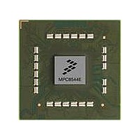
MPC8544DS Freescale Semiconductor, MPC8544DS Datasheet - Page 652

MPC8544DS
Manufacturer Part Number
MPC8544DS
Description
BOARD DEVELOPMENT SYSTEM 8544
Manufacturer
Freescale Semiconductor
Series
PowerQUICC III™r
Type
MPUr
Datasheets
1.MPC8544VTALF.pdf
(117 pages)
2.MPC8544VTALF.pdf
(2 pages)
3.MPC8544VTALF.pdf
(1340 pages)
4.MPC8544DS.pdf
(2 pages)
Specifications of MPC8544DS
Contents
Board
Processor To Be Evaluated
MPC8544E
Data Bus Width
32 bit
Interface Type
Ethernet, I2C
Operating Supply Voltage
- 0.3 V to + 1.1 V
Leaded Process Compatible
Yes
Peak Reflow Compatible (260 C)
Yes
Rohs Compliant
Yes
For Use With/related Products
MPC8544
For Use With
PPC8544EVTANG - EVAL MPC8544 783FCPBGA
Lead Free Status / RoHS Status
Lead free / RoHS Compliant
- MPC8544VTALF PDF datasheet
- MPC8544VTALF PDF datasheet #2
- MPC8544VTALF PDF datasheet #3
- MPC8544DS PDF datasheet #4
- Current page: 652 of 1340
- Download datasheet (12Mb)
Local Bus Controller
14.4
The LBC allows the implementation of memory systems with very specific timing requirements.
Each memory bank (chip select) can be assigned to any one of these three type of machines through the
machine select bits of the base register for that bank (BRn[MSEL]), as illustrated in
match occurs, the corresponding machine (GPCM, SDRAM or UPM) then takes ownership of the external
signals that control the access and maintains control until the transaction ends.
14-32
•
•
•
The SDRAM machine provides an interface to SDRAMs using bank interleaving and back-to-back
page mode to achieve high performance through a multiplexed address/data bus. An internal PLL
for bus clock generation ensures improved data set-up margins for board designs.
The GPCM provides interfacing for simpler, lower-performance memories and memory-mapped
devices. It has inherently lower performance because it does not support bursting. For this reason,
GPCM-controlled banks are used primarily for boot-loading and access to low-performance
memory-mapped peripherals.
The UPM supports refresh timers, address multiplexing of the external bus and generation of
programmable control signals for row address and column address strobes, to allow for a minimal
glue logic interface to DRAMs, burstable SRAMs, and almost any other kind of peripheral. The
UPM can be used to generate flexible, user-defined timing patterns for control signals that govern
a memory device. These patterns define how the external control signals behave during a read,
write, burst-read, or burst-write access. Refresh timers are also available to periodically initiate
user-defined refresh patterns.
Functional Description
MPC8544E PowerQUICC III Integrated Host Processor Family Reference Manual, Rev. 1
Bank Select
Comparator
Address
MSEL
Field
Figure 14-20. Basic Operation of Memory Controllers in the LBC
32-Bit Physical
RAM Address (A)
34-bit System
Address
Internal Memory Access Request Select
SDRAM Machine
External Signals
UPM A/B/C
Generator
Signals
Timing
MUX
GPCM
Figure
Freescale Semiconductor
14-20. If a bank
Related parts for MPC8544DS
Image
Part Number
Description
Manufacturer
Datasheet
Request
R
Part Number:
Description:
Manufacturer:
Freescale Semiconductor, Inc
Datasheet:
Part Number:
Description:
Manufacturer:
Freescale Semiconductor, Inc
Datasheet:
Part Number:
Description:
Manufacturer:
Freescale Semiconductor, Inc
Datasheet:
Part Number:
Description:
Manufacturer:
Freescale Semiconductor, Inc
Datasheet:
Part Number:
Description:
Manufacturer:
Freescale Semiconductor, Inc
Datasheet:
Part Number:
Description:
Manufacturer:
Freescale Semiconductor, Inc
Datasheet:
Part Number:
Description:
Manufacturer:
Freescale Semiconductor, Inc
Datasheet:
Part Number:
Description:
Manufacturer:
Freescale Semiconductor, Inc
Datasheet:
Part Number:
Description:
Manufacturer:
Freescale Semiconductor, Inc
Datasheet:
Part Number:
Description:
Manufacturer:
Freescale Semiconductor, Inc
Datasheet:
Part Number:
Description:
Manufacturer:
Freescale Semiconductor, Inc
Datasheet:
Part Number:
Description:
Manufacturer:
Freescale Semiconductor, Inc
Datasheet:
Part Number:
Description:
Manufacturer:
Freescale Semiconductor, Inc
Datasheet:
Part Number:
Description:
Manufacturer:
Freescale Semiconductor, Inc
Datasheet:
Part Number:
Description:
Manufacturer:
Freescale Semiconductor, Inc
Datasheet:


