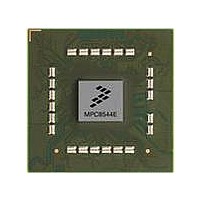
MPC8544DS Freescale Semiconductor, MPC8544DS Datasheet - Page 685

MPC8544DS
Manufacturer Part Number
MPC8544DS
Description
BOARD DEVELOPMENT SYSTEM 8544
Manufacturer
Freescale Semiconductor
Series
PowerQUICC III™r
Type
MPUr
Datasheets
1.MPC8544VTALF.pdf
(117 pages)
2.MPC8544VTALF.pdf
(2 pages)
3.MPC8544VTALF.pdf
(1340 pages)
4.MPC8544DS.pdf
(2 pages)
Specifications of MPC8544DS
Contents
Board
Processor To Be Evaluated
MPC8544E
Data Bus Width
32 bit
Interface Type
Ethernet, I2C
Operating Supply Voltage
- 0.3 V to + 1.1 V
Leaded Process Compatible
Yes
Peak Reflow Compatible (260 C)
Yes
Rohs Compliant
Yes
For Use With/related Products
MPC8544
For Use With
PPC8544EVTANG - EVAL MPC8544 783FCPBGA
Lead Free Status / RoHS Status
Lead free / RoHS Compliant
- MPC8544VTALF PDF datasheet
- MPC8544VTALF PDF datasheet #2
- MPC8544VTALF PDF datasheet #3
- MPC8544DS PDF datasheet #4
- Current page: 685 of 1340
- Download datasheet (12Mb)
14.4.4.4.1
The RAM word is a 32-bit microinstruction stored in one of 64 locations in the RAM array. It specifies
timing for external signals controlled by the UPM.
and BSTn bits determine the state of UPM signals LCSn and LBS[0:3] at each quarter phase of the bus
clock.
Table 14-28
Freescale Semiconductor
10–11
Bits
8–9
12
0
1
2
3
4
5
6
7
Reset
Reset
W
W
R
R
CST1 CST2
G3T1 G3T3
16
0
Name
CST1
CST2
CST3
CST4
BST1
BST2
BST3
BST4
G1T1
G0H
G0L
describes RAM word fields.
MPC8544E PowerQUICC III Integrated Host Processor Family Reference Manual, Rev. 1
17
RAM Words
1
G4T1/DLT
Chip select timing 1. Defines the state (0 or 1) of LCS n during bus clock quarter phase 1.
Chip select timing 2. Defines the state (0 or 1) of LCS n during bus clock quarter phase 2.
Chip select timing 3. Defines the state (0 or 1) of LCS n during bus clock quarter phase 3.
Chip select timing 4. Defines the state (0 or 1) of LCS n during bus clock quarter phase 4.
Byte select timing 1. Defines the state (0 or 1) of LBS during bus clock quarter phase 1.
Byte select timing 2:. Defines the state (0 or 1) of LBS during bus clock quarter phase 2.
Byte select timing 3. Defines the state (0 or 1) of LBS during bus clock quarter phase 3.
Byte select timing 4. Defines the state (0 or 1) of LBS during bus clock quarter phase 4.
General-purpose line 0 lower. Defines the state of LGPL0 during the bus clock quarter phases 1 and
2 (first half phase).
00 Value defined by M x MR[G0CL]
01 Reserved
10 0
11 1
General-purpose line 0 higher. Defines the state of LGPL0 during the bus clock quarter phases 3 and
4 (second half phase).
00 Value defined by M x MR[G0CL]
01 Reserved
10 0
11 1
General-purpose line 1 timing 1. Defines the state (0 or 1) of LGPL1 during bus clock quarter phases
1 and 2 (first half phase).
CST3
18
3
2
G4T3/WAEN G5T1 G5T3
Figure 14-58. RAM Word Field Descriptions
Table 14-28. RAM Word Field Descriptions
CST4
19
3
BST1 BST2 BST3 BST4
20
4
21
5
Figure 14-58
All zeros
All zeros
22
6
REDO
Description
23
7
shows the RAM word fields. The CSTn
LOOP EXEN AMX
24
8
G0L
25
9
10 11
26 27
G0H G1T1 G1T3 G2T1 G2T3
NA
12
28
Access: Read/Write
Local Bus Controller
UTA TODT LAST
13
29
14
30
14-65
15
31
Related parts for MPC8544DS
Image
Part Number
Description
Manufacturer
Datasheet
Request
R
Part Number:
Description:
Manufacturer:
Freescale Semiconductor, Inc
Datasheet:
Part Number:
Description:
Manufacturer:
Freescale Semiconductor, Inc
Datasheet:
Part Number:
Description:
Manufacturer:
Freescale Semiconductor, Inc
Datasheet:
Part Number:
Description:
Manufacturer:
Freescale Semiconductor, Inc
Datasheet:
Part Number:
Description:
Manufacturer:
Freescale Semiconductor, Inc
Datasheet:
Part Number:
Description:
Manufacturer:
Freescale Semiconductor, Inc
Datasheet:
Part Number:
Description:
Manufacturer:
Freescale Semiconductor, Inc
Datasheet:
Part Number:
Description:
Manufacturer:
Freescale Semiconductor, Inc
Datasheet:
Part Number:
Description:
Manufacturer:
Freescale Semiconductor, Inc
Datasheet:
Part Number:
Description:
Manufacturer:
Freescale Semiconductor, Inc
Datasheet:
Part Number:
Description:
Manufacturer:
Freescale Semiconductor, Inc
Datasheet:
Part Number:
Description:
Manufacturer:
Freescale Semiconductor, Inc
Datasheet:
Part Number:
Description:
Manufacturer:
Freescale Semiconductor, Inc
Datasheet:
Part Number:
Description:
Manufacturer:
Freescale Semiconductor, Inc
Datasheet:
Part Number:
Description:
Manufacturer:
Freescale Semiconductor, Inc
Datasheet:


