MCF5407CAI220 Freescale Semiconductor, MCF5407CAI220 Datasheet - Page 12
MCF5407CAI220
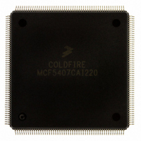
Manufacturer Part Number
MCF5407CAI220
Description
IC MPU 32B 220MHZ COLDF 208-FQFP
Manufacturer
Freescale Semiconductor
Series
MCF540xr
Specifications of MCF5407CAI220
Core Processor
Coldfire V4
Core Size
32-Bit
Speed
220MHz
Connectivity
EBI/EMI, I²C, UART/USART
Peripherals
DMA, WDT
Number Of I /o
16
Program Memory Type
ROMless
Ram Size
4K x 8
Voltage - Supply (vcc/vdd)
1.65 V ~ 3.6 V
Oscillator Type
External
Operating Temperature
-40°C ~ 85°C
Package / Case
208-FQFP
Processor Series
MCF540x
Core
ColdFire V4
Data Bus Width
32 bit
Program Memory Size
8 KB
Data Ram Size
4 KB
Maximum Clock Frequency
162 MHz
Number Of Programmable I/os
16
Operating Supply Voltage
1.8 V to 3.3 V
Mounting Style
SMD/SMT
3rd Party Development Tools
JLINK-CF-BDM26, EWCF
Cpu Speed
220MHz
Embedded Interface Type
I2C, UART
Digital Ic Case Style
FQFP
No. Of Pins
208
Supply Voltage Range
3.3V
Rohs Compliant
Yes
For Use With
M5407C3 - KIT EVAL FOR MCF5407 W/ETHERNET
Lead Free Status / RoHS Status
Lead free / RoHS Compliant
Eeprom Size
-
Program Memory Size
-
Data Converters
-
Lead Free Status / Rohs Status
Lead free / RoHS Compliant
Available stocks
Company
Part Number
Manufacturer
Quantity
Price
Company:

Part Number:
MCF5407CAI220
Manufacturer:
Freescale
Quantity:
789
Company:
Part Number:
MCF5407CAI220
Manufacturer:
Freescale Semiconductor
Quantity:
10 000


Paragraph
Number
11.1
11.1.1
11.1.2
11.2
11.2.1
11.3
11.3.1
11.3.2
11.3.2.1
11.3.2.2
11.3.2.3
11.3.3
11.3.3.1
11.3.3.2
11.3.3.3
11.3.3.4
11.3.3.5
11.4
11.4.1
11.4.2
11.4.3
11.4.3.1
11.4.3.2
11.4.3.3
11.4.4
11.4.4.1
11.4.4.2
11.4.4.3
11.4.4.4
11.4.4.5
11.4.4.6
11.4.5
11.4.5.1
11.5
11.5.1
11.5.2
11.5.3
11.5.4
11.5.5
11.5.6
xii
Overview........................................................................................................... 11-1
DRAM Controller Operation ............................................................................ 11-3
Asynchronous Operation .................................................................................. 11-4
Synchronous Operation................................................................................... 11-16
SDRAM Example ........................................................................................... 11-34
Definitions .................................................................................................... 11-2
Block Diagram and Major Components ....................................................... 11-2
DRAM Controller Registers ......................................................................... 11-3
DRAM Controller Signals in Asynchronous Mode...................................... 11-4
Asynchronous Register Set........................................................................... 11-4
General Asynchronous Operation Guidelines .............................................. 11-8
DRAM Controller Signals in Synchronous Mode...................................... 11-17
Using Edge Select (EDGESEL) ................................................................. 11-18
Synchronous Register Set ........................................................................... 11-19
General Synchronous Operation Guidelines............................................... 11-23
Initialization Sequence................................................................................ 11-32
SDRAM Interface Configuration................................................................ 11-34
DCR Initialization....................................................................................... 11-35
DACR Initialization.................................................................................... 11-35
DMR Initialization...................................................................................... 11-37
Mode Register Initialization ....................................................................... 11-38
Initialization Code....................................................................................... 11-39
DRAM Control Register (DCR) in Asynchronous Mode ........................ 11-4
DRAM Address and Control Registers (DACR0/DACR1) ..................... 11-5
DRAM Controller Mask Registers (DMR0/DMR1) ................................ 11-7
Non-Page-Mode Operation..................................................................... 11-11
Burst Page-Mode Operation ................................................................... 11-12
Continuous Page Mode........................................................................... 11-13
Extended Data Out (EDO) Operation..................................................... 11-15
Refresh Operation ................................................................................... 11-16
DRAM Control Register (DCR) in Synchronous Mode......................... 11-19
DRAM Address and Control Registers (DACR0/DACR1)
DRAM Controller Mask Registers (DMR0/DMR1) .............................. 11-22
Address Multiplexing ............................................................................. 11-23
Interfacing Example................................................................................ 11-27
Burst Page Mode..................................................................................... 11-27
Continuous Page Mode........................................................................... 11-29
Auto-Refresh Operation.......................................................................... 11-31
Self-Refresh Operation ........................................................................... 11-32
Mode Register Settings........................................................................... 11-33
in Synchronous Mode ......................................................................... 11-20
MCF5407 User’s Manual
CONTENTS
Title
Number
Page
Related parts for MCF5407CAI220
Image
Part Number
Description
Manufacturer
Datasheet
Request
R

Part Number:
Description:
Mcf5407 Coldfire Integrated Microprocessor User
Manufacturer:
Freescale Semiconductor, Inc
Datasheet:
Part Number:
Description:
Manufacturer:
Freescale Semiconductor, Inc
Datasheet:
Part Number:
Description:
Manufacturer:
Freescale Semiconductor, Inc
Datasheet:
Part Number:
Description:
Manufacturer:
Freescale Semiconductor, Inc
Datasheet:
Part Number:
Description:
Manufacturer:
Freescale Semiconductor, Inc
Datasheet:
Part Number:
Description:
Manufacturer:
Freescale Semiconductor, Inc
Datasheet:
Part Number:
Description:
Manufacturer:
Freescale Semiconductor, Inc
Datasheet:
Part Number:
Description:
Manufacturer:
Freescale Semiconductor, Inc
Datasheet:
Part Number:
Description:
Manufacturer:
Freescale Semiconductor, Inc
Datasheet:
Part Number:
Description:
Manufacturer:
Freescale Semiconductor, Inc
Datasheet:
Part Number:
Description:
Manufacturer:
Freescale Semiconductor, Inc
Datasheet:
Part Number:
Description:
Manufacturer:
Freescale Semiconductor, Inc
Datasheet:
Part Number:
Description:
Manufacturer:
Freescale Semiconductor, Inc
Datasheet:
Part Number:
Description:
Manufacturer:
Freescale Semiconductor, Inc
Datasheet:
Part Number:
Description:
Manufacturer:
Freescale Semiconductor, Inc
Datasheet: