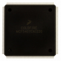
MCF5407CAI220 Freescale Semiconductor, MCF5407CAI220 Datasheet - Page 158

MCF5407CAI220
Manufacturer Part Number
MCF5407CAI220
Description
IC MPU 32B 220MHZ COLDF 208-FQFP
Manufacturer
Freescale Semiconductor
Series
MCF540xr
Specifications of MCF5407CAI220
Core Processor
Coldfire V4
Core Size
32-Bit
Speed
220MHz
Connectivity
EBI/EMI, I²C, UART/USART
Peripherals
DMA, WDT
Number Of I /o
16
Program Memory Type
ROMless
Ram Size
4K x 8
Voltage - Supply (vcc/vdd)
1.65 V ~ 3.6 V
Oscillator Type
External
Operating Temperature
-40°C ~ 85°C
Package / Case
208-FQFP
Processor Series
MCF540x
Core
ColdFire V4
Data Bus Width
32 bit
Program Memory Size
8 KB
Data Ram Size
4 KB
Maximum Clock Frequency
162 MHz
Number Of Programmable I/os
16
Operating Supply Voltage
1.8 V to 3.3 V
Mounting Style
SMD/SMT
3rd Party Development Tools
JLINK-CF-BDM26, EWCF
Cpu Speed
220MHz
Embedded Interface Type
I2C, UART
Digital Ic Case Style
FQFP
No. Of Pins
208
Supply Voltage Range
3.3V
Rohs Compliant
Yes
For Use With
M5407C3 - KIT EVAL FOR MCF5407 W/ETHERNET
Lead Free Status / RoHS Status
Lead free / RoHS Compliant
Eeprom Size
-
Program Memory Size
-
Data Converters
-
Lead Free Status / Rohs Status
Lead free / RoHS Compliant
Available stocks
Company
Part Number
Manufacturer
Quantity
Price
Company:
Part Number:
MCF5407CAI220
Manufacturer:
Freescale
Quantity:
789
Company:
Part Number:
MCF5407CAI220
Manufacturer:
Freescale Semiconductor
Quantity:
10 000
- Current page: 158 of 546
- Download datasheet (7Mb)
Signal Descriptions
The Version 2 ColdFire core implemented the original debug architecture, now called
Revision A. Based on feedback from customers and third-party developers, enhancements
have been added to succeeding generations of ColdFire cores. The Version 3 core
implements the Revision B of the debug architecture, providing more flexibility for
configuring the hardware breakpoint trigger registers and removing the restrictions
involving concurrent BDM processing while hardware breakpoint registers are active.
The MCF5407 core implements Revision C of the debug architecture, which more than
doubles the on-chip breakpoint registers and provides an ability to interrupt debug service
routines. For Revision C, the revision level bit, CSR[HRL], is 2. See Section 5.4.4,
“Configuration/Status Register (CSR).”
5.2 Signal Descriptions
Table 5-1 describes debug module signals. All ColdFire debug signals are unidirectional
and related to a rising edge of the processor core’s clock signal. The standard 26-pin debug
connector is shown in Section 5.7, “Motorola-Recommended BDM Pinout.”
Development Serial
Clock (DSCLK)
Development Serial
Input (DSI)
Development Serial
Output (DSO)
Breakpoint (BKPT)
Processor Status
Clock (PSTCLK)
Processor
Status/Debug Data
(PSTDDATA[7:0])
5-2
Signal
Internally synchronized input that clocks the serial communication port to the debug module.
Maximum frequency is 1/5 the processor CLK speed. At the synchronized rising edge of
DSCLK, the data input on DSI is sampled and DSO changes state. The logic level on DSCLK is
validated if it has the same value on two consecutive rising CLKIN edges.
Internally synchronized input that provides data input for the serial communication port to the
debug module.
Provides serial output communication for debug module responses. DSO is registered
internally.
Used to request a manual breakpoint. Assertion of BKPT puts the processor into a halted state
after the current instruction completes. Halt status is reflected on processor status/debug data
signals (PSTDDATA[7:0]) as the value 0xF. If CSR[BKD] is set (disabling normal BKPT
functionality), asserting BKPT generates a debug interrupt exception in the processor.
Half-speed version of the processor clock. Its rising edge appears in the center of the two
processor-cycle window of valid PSTDDATA output. See Figure 5-2. Because debug trace port
signals change on alternate processor cycles and are unrelated to external bus frequency,
PSTCLK helps the development system sample PSTDDATA values.
If real-time trace is not used, setting CSR[PCD] keeps PSTCLK and PSTDDATA outputs from
toggling without disabling triggers. Non-quiescent operation can be reenabled by clearing
CSR[PCD], although the emulator must resynchronize with the PSTDDATA output.
PSTCLK starts clocking only when the first non-zero PST value (0xC, 0xD, or 0xF) occurs
during system reset exception processing. Table 5-4 describes PST values. Chapter 7,
“Phase-Locked Loop (PLL),” describes PSTCLK generation.
These outputs indicate both processor status and captured address and data values and are
discussed more thoroughly in Section 5.2.1, “Processor Status/Debug Data (PSTDDATA[7:0]).
Table 5-1. Debug Module Signals
MCF5407 User’s Manual
Description
Related parts for MCF5407CAI220
Image
Part Number
Description
Manufacturer
Datasheet
Request
R
Part Number:
Description:
Mcf5407 Coldfire Integrated Microprocessor User
Manufacturer:
Freescale Semiconductor, Inc
Datasheet:
Part Number:
Description:
Manufacturer:
Freescale Semiconductor, Inc
Datasheet:
Part Number:
Description:
Manufacturer:
Freescale Semiconductor, Inc
Datasheet:
Part Number:
Description:
Manufacturer:
Freescale Semiconductor, Inc
Datasheet:
Part Number:
Description:
Manufacturer:
Freescale Semiconductor, Inc
Datasheet:
Part Number:
Description:
Manufacturer:
Freescale Semiconductor, Inc
Datasheet:
Part Number:
Description:
Manufacturer:
Freescale Semiconductor, Inc
Datasheet:
Part Number:
Description:
Manufacturer:
Freescale Semiconductor, Inc
Datasheet:
Part Number:
Description:
Manufacturer:
Freescale Semiconductor, Inc
Datasheet:
Part Number:
Description:
Manufacturer:
Freescale Semiconductor, Inc
Datasheet:
Part Number:
Description:
Manufacturer:
Freescale Semiconductor, Inc
Datasheet:
Part Number:
Description:
Manufacturer:
Freescale Semiconductor, Inc
Datasheet:
Part Number:
Description:
Manufacturer:
Freescale Semiconductor, Inc
Datasheet:
Part Number:
Description:
Manufacturer:
Freescale Semiconductor, Inc
Datasheet:
Part Number:
Description:
Manufacturer:
Freescale Semiconductor, Inc
Datasheet:


