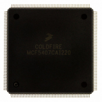
MCF5407CAI220 Freescale Semiconductor, MCF5407CAI220 Datasheet - Page 351

MCF5407CAI220
Manufacturer Part Number
MCF5407CAI220
Description
IC MPU 32B 220MHZ COLDF 208-FQFP
Manufacturer
Freescale Semiconductor
Series
MCF540xr
Specifications of MCF5407CAI220
Core Processor
Coldfire V4
Core Size
32-Bit
Speed
220MHz
Connectivity
EBI/EMI, I²C, UART/USART
Peripherals
DMA, WDT
Number Of I /o
16
Program Memory Type
ROMless
Ram Size
4K x 8
Voltage - Supply (vcc/vdd)
1.65 V ~ 3.6 V
Oscillator Type
External
Operating Temperature
-40°C ~ 85°C
Package / Case
208-FQFP
Processor Series
MCF540x
Core
ColdFire V4
Data Bus Width
32 bit
Program Memory Size
8 KB
Data Ram Size
4 KB
Maximum Clock Frequency
162 MHz
Number Of Programmable I/os
16
Operating Supply Voltage
1.8 V to 3.3 V
Mounting Style
SMD/SMT
3rd Party Development Tools
JLINK-CF-BDM26, EWCF
Cpu Speed
220MHz
Embedded Interface Type
I2C, UART
Digital Ic Case Style
FQFP
No. Of Pins
208
Supply Voltage Range
3.3V
Rohs Compliant
Yes
For Use With
M5407C3 - KIT EVAL FOR MCF5407 W/ETHERNET
Lead Free Status / RoHS Status
Lead free / RoHS Compliant
Eeprom Size
-
Program Memory Size
-
Data Converters
-
Lead Free Status / Rohs Status
Lead free / RoHS Compliant
Available stocks
Company
Part Number
Manufacturer
Quantity
Price
Company:
Part Number:
MCF5407CAI220
Manufacturer:
Freescale
Quantity:
789
Company:
Part Number:
MCF5407CAI220
Manufacturer:
Freescale Semiconductor
Quantity:
10 000
- Current page: 351 of 546
- Download datasheet (7Mb)
14.3.4 Modem Control Register (MODCTL)
The modem control register (MODCTL), Figure 14-5, controls whether UART1 is in
UART mode or in one of three modem modes.
Table 14-5 describes MODCTL fields.
Bits
5–4
1–0
Address
7
6
3
2
Reset
Field
R/W
SHDIR
MODE
Name
ACRB
DTS1
AWR
DSL
Table 14-5. Modem Control Register (MODCTL) Field Descriptions
ACRB
AC ‘97 cold reset (active low).
0 The genera-purpose I/O used as the AC ‘97 cold reset output pin is active
1 The genera-purpose I/O used as the AC ‘97 cold reset output pin is inactive
AC ‘97 warm reset (active high)
0 Warm reset is inactive, letting UART1’s RTS output to function normally as the AC ‘97 frame
1 Forces a 1 on UART1’s RTS output, which is used as the AC ‘97 frame sync.
Channel select for DMA channels 2 and 3. The sources for the interrupt request lines that drive
DMA DREQ[3:2] are selected by multiplexers in UART1, which are controlled by DSL.
00 DMA DREQ2 is driven by UART0 combined Tx/Rx interrupt
01 DMA DREQ2 is driven by UART1 Rx interrupt
10 same as 00
11 DMA DREQ2 is driven by UART1 Rx interrupt
When UART1 uses both DREQ lines, DREQ3 and DREQ2 are driven by the Tx FIFO empty and Rx
FIFO full conditions, respectively. The Rx FIFO not-empty condition can be used instead of Rx FIFO
full by clearing UMR1n[6]. UART0 and UART1 have separate request lines to the interrupt
controller. Each is sourced from the combined Tx/Rx interrupt from the associated UART.
Delay of time slot 1. Determines the starting point of the first bit of the first time slot of a new frame.
0 The rising edge of frame sync
1 One bit-clock cycle after the rising edge of frame sync
Shift direction. For AC ‘97 this bit must be 0.
0 Samples/time slots are transferred msb first
1 Samples/time slots are transferred lsb first
Mode select for UART1.
00 UART mode (default mode after hard reset). Changing from modem mode back to UART mode
01 8-bit CODEC interface mode
10 16-bit CODEC interface mode
11 AC ‘97 mode
7
sync.
DMA DREQ3 is driven by UART1 combined Tx/Rx interrupt
DMA DREQ3 is driven by UART1 Tx interrupt
DMA DREQ3 is driven by UART1 combined Tx/Rx interrupt. This combination is a by-product of
implementation and may not be useful.
by writing 00 to this field has the same effect on UART1 as a hard reset—all registers and
control logic are reset and the Tx and Rx FIFO pointers are reinitialized, effectively emptying the
FIFOs.
Figure 14-5. Modem Control Register (MODCTL)
AWR
6
Chapter 14. UART Modules
5
DSL
MBAR + 0x202
1000_0000
4
Description
R/W
DTS1
3
SHDIR
2
Register Descriptions
1
MODE
0
14-9
Related parts for MCF5407CAI220
Image
Part Number
Description
Manufacturer
Datasheet
Request
R
Part Number:
Description:
Mcf5407 Coldfire Integrated Microprocessor User
Manufacturer:
Freescale Semiconductor, Inc
Datasheet:
Part Number:
Description:
Manufacturer:
Freescale Semiconductor, Inc
Datasheet:
Part Number:
Description:
Manufacturer:
Freescale Semiconductor, Inc
Datasheet:
Part Number:
Description:
Manufacturer:
Freescale Semiconductor, Inc
Datasheet:
Part Number:
Description:
Manufacturer:
Freescale Semiconductor, Inc
Datasheet:
Part Number:
Description:
Manufacturer:
Freescale Semiconductor, Inc
Datasheet:
Part Number:
Description:
Manufacturer:
Freescale Semiconductor, Inc
Datasheet:
Part Number:
Description:
Manufacturer:
Freescale Semiconductor, Inc
Datasheet:
Part Number:
Description:
Manufacturer:
Freescale Semiconductor, Inc
Datasheet:
Part Number:
Description:
Manufacturer:
Freescale Semiconductor, Inc
Datasheet:
Part Number:
Description:
Manufacturer:
Freescale Semiconductor, Inc
Datasheet:
Part Number:
Description:
Manufacturer:
Freescale Semiconductor, Inc
Datasheet:
Part Number:
Description:
Manufacturer:
Freescale Semiconductor, Inc
Datasheet:
Part Number:
Description:
Manufacturer:
Freescale Semiconductor, Inc
Datasheet:
Part Number:
Description:
Manufacturer:
Freescale Semiconductor, Inc
Datasheet:


