MCF5407CAI220 Freescale Semiconductor, MCF5407CAI220 Datasheet - Page 23
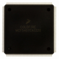
MCF5407CAI220
Manufacturer Part Number
MCF5407CAI220
Description
IC MPU 32B 220MHZ COLDF 208-FQFP
Manufacturer
Freescale Semiconductor
Series
MCF540xr
Specifications of MCF5407CAI220
Core Processor
Coldfire V4
Core Size
32-Bit
Speed
220MHz
Connectivity
EBI/EMI, I²C, UART/USART
Peripherals
DMA, WDT
Number Of I /o
16
Program Memory Type
ROMless
Ram Size
4K x 8
Voltage - Supply (vcc/vdd)
1.65 V ~ 3.6 V
Oscillator Type
External
Operating Temperature
-40°C ~ 85°C
Package / Case
208-FQFP
Processor Series
MCF540x
Core
ColdFire V4
Data Bus Width
32 bit
Program Memory Size
8 KB
Data Ram Size
4 KB
Maximum Clock Frequency
162 MHz
Number Of Programmable I/os
16
Operating Supply Voltage
1.8 V to 3.3 V
Mounting Style
SMD/SMT
3rd Party Development Tools
JLINK-CF-BDM26, EWCF
Cpu Speed
220MHz
Embedded Interface Type
I2C, UART
Digital Ic Case Style
FQFP
No. Of Pins
208
Supply Voltage Range
3.3V
Rohs Compliant
Yes
For Use With
M5407C3 - KIT EVAL FOR MCF5407 W/ETHERNET
Lead Free Status / RoHS Status
Lead free / RoHS Compliant
Eeprom Size
-
Program Memory Size
-
Data Converters
-
Lead Free Status / Rohs Status
Lead free / RoHS Compliant
Available stocks
Company
Part Number
Manufacturer
Quantity
Price
Company:

Part Number:
MCF5407CAI220
Manufacturer:
Freescale
Quantity:
789
Company:
Part Number:
MCF5407CAI220
Manufacturer:
Freescale Semiconductor
Quantity:
10 000


Figure
Number
6-4
6-5
6-6
6-7
6-8
6-9
6-10
6-11
6-12
6-13
7-1
7-2
7-3
7-4
7-5
8-1
8-2
8-3
8-4
8-5
8-6
8-7
8-8
8-9
8-10
9-1
9-2
9-3
9-4
9-5
10-1
10-2
10-3
10-4
11-1
11-2
11-3
11-4
11-5
11-6
11-7
11-8
11-9
MCF5407 Embedded System Recovery from Unterminated Access........................... 6-7
Pin Assignment Register (PAR) ................................................................................. 6-10
Default Bus Master Register (MPARK) ..................................................................... 6-11
Round Robin Arbitration (PARK = 00)...................................................................... 6-12
Park on Master Core Priority (PARK = 01) ............................................................... 6-13
Park on DMA Module Priority (PARK = 10)............................................................. 6-13
Park on Current Master Priority (PARK = 01) ........................................................... 6-14
PLL Module Block Diagram ........................................................................................ 7-1
PLL Control Register (PLLCR).................................................................................... 7-3
CLKIN, PCLK, PSTCLK, and BCLKO Timing .......................................................... 7-5
Reset and Initialization Timing..................................................................................... 7-6
I
I
Repeated START .......................................................................................................... 8-4
Synchronized Clock SCL.............................................................................................. 8-5
I
I
I
I
I
Flow-Chart of Typical I2C Interrupt Routine............................................................. 8-14
Interrupt Controller Block Diagram.............................................................................. 9-1
Interrupt Control Registers (ICR0–ICR9) .................................................................... 9-3
Autovector Register (AVR) .......................................................................................... 9-5
Interrupt Pending Register (IPR) and Interrupt Mask Register (IMR) ......................... 9-7
Interrupt Port Assignment Register (IRQPAR) ............................................................ 9-7
Connections for External Memory Port Sizes ............................................................ 10-4
Chip Select Address Registers (CSAR0–CSAR7) ..................................................... 10-6
Chip Select Mask Registers (CSMRn) ....................................................................... 10-7
Chip-Select Control Registers (CSCR0–CSCR7) ...................................................... 10-8
Asynchronous/Synchronous DRAM Controller Block Diagram ............................... 11-2
DRAM Control Register (DCR) (Asynchronous Mode) ............................................ 11-5
DRAM Address and Control Registers (DACR0/DACR1)........................................ 11-6
DRAM Controller Mask Registers (DMR0 and DMR1)............................................ 11-7
Basic Non-Page-Mode Operation RCD = 0, RNCN = 1 (4-4-4-4) .......................... 11-11
Basic Non-Page-Mode Operation RCD = 1, RNCN = 0 (5-5-5-5) .......................... 11-12
Burst Page-Mode Read Operation (4-3-3-3)............................................................. 11-13
Burst Page-Mode Write Operation (4-3-3-3)............................................................ 11-13
Continuous Page-Mode Operation............................................................................ 11-14
System Protection Control Register (SYPCR) ............................................................ 6-8
Software Watchdog Interrupt Vector Register (SWIVR)............................................ 6-9
Software Watchdog Service Register (SWSR)............................................................ 6-9
PLL Power Supply Filter Circuit ................................................................................. 7-6
2
2
2
2
2
2
2
C Module Block Diagram .......................................................................................... 8-2
C Standard Communication Protocol ........................................................................ 8-3
C Address Register (IADR) ....................................................................................... 8-6
C Frequency Divider Register (IFDR)....................................................................... 8-7
C Control Register (I2CR) ......................................................................................... 8-8
CR Status Register (I2SR) ......................................................................................... 8-9
C Data I/O Register (I2DR) ..................................................................................... 8-10
ILLUSTRATIONS
Illustrations
Title
Number
Page
xxiii
Related parts for MCF5407CAI220
Image
Part Number
Description
Manufacturer
Datasheet
Request
R

Part Number:
Description:
Mcf5407 Coldfire Integrated Microprocessor User
Manufacturer:
Freescale Semiconductor, Inc
Datasheet:
Part Number:
Description:
Manufacturer:
Freescale Semiconductor, Inc
Datasheet:
Part Number:
Description:
Manufacturer:
Freescale Semiconductor, Inc
Datasheet:
Part Number:
Description:
Manufacturer:
Freescale Semiconductor, Inc
Datasheet:
Part Number:
Description:
Manufacturer:
Freescale Semiconductor, Inc
Datasheet:
Part Number:
Description:
Manufacturer:
Freescale Semiconductor, Inc
Datasheet:
Part Number:
Description:
Manufacturer:
Freescale Semiconductor, Inc
Datasheet:
Part Number:
Description:
Manufacturer:
Freescale Semiconductor, Inc
Datasheet:
Part Number:
Description:
Manufacturer:
Freescale Semiconductor, Inc
Datasheet:
Part Number:
Description:
Manufacturer:
Freescale Semiconductor, Inc
Datasheet:
Part Number:
Description:
Manufacturer:
Freescale Semiconductor, Inc
Datasheet:
Part Number:
Description:
Manufacturer:
Freescale Semiconductor, Inc
Datasheet:
Part Number:
Description:
Manufacturer:
Freescale Semiconductor, Inc
Datasheet:
Part Number:
Description:
Manufacturer:
Freescale Semiconductor, Inc
Datasheet:
Part Number:
Description:
Manufacturer:
Freescale Semiconductor, Inc
Datasheet: